

Lattice Semiconductor
LCMXO2-256HC-5SG48I
FPGAs

Not available to buy online? Want the lower wholesale price? Please Send RFQ to get best price, we will respond immediately


.png?x-oss-process=image/format,webp/resize,p_30)


LCMXO2-256HC-5SG48I Description
The LCMXO2-256HC-5SG48I is a field programmable gate array (FPGA) device manufactured by Lattice Semiconductor. This device belongs to the LatticeECP2 series of FPGAs, which are known for their low power consumption, high performance, and small form factor.
Description:
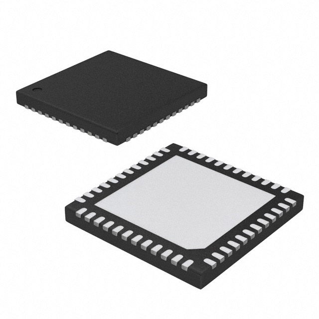
The LCMXO2-256HC-5SG48I is a mid-range FPGA that offers a balance between performance and power efficiency. It features a 256-macrocell array, which provides a high level of programmability and flexibility for a wide range of applications. The device is available in a 5x5 mm QFN package, making it suitable for compact and space-constrained designs.
Features:
- Low power consumption: The LatticeECP2 series of FPGAs are designed for low power applications, making them ideal for battery-powered or energy-sensitive systems.
- High performance: The LCMXO2-256HC-5SG48I offers high-speed performance, with support for high-frequency clocking and fast I/O interfaces.
- Small form factor: The 5x5 mm QFN package allows for compact and space-efficient designs, making it suitable for portable or embedded applications.
- Versatile I/O options: The device supports a wide range of I/O standards, making it compatible with various peripherals and interfaces.
- Security features: The LCMXO2-256HC-5SG48I includes security features such as encryption and secure boot, ensuring the protection of sensitive data and intellectual property.
- Easy programmability: The device can be easily programmed using Lattice's development tools and software, allowing for fast and efficient design implementation.
Applications:
The LCMXO2-256HC-5SG48I is suitable for a wide range of applications, including but not limited to:
- Industrial control systems: The device's low power consumption and high performance make it ideal for industrial control applications, such as motor control and sensor interfacing.
- Consumer electronics: The compact form factor and versatile I/O options make it suitable for consumer electronics, such as wearable devices and portable gadgets.
- Communication systems: The high-speed performance and support for various communication protocols make it suitable for communication systems, such as wireless transceivers and network interface cards.
- Automotive applications: The device's robustness and security features make it suitable for automotive applications, such as infotainment systems and advanced driver assistance systems (ADAS).
- Medical devices: The LCMXO2-256HC-5SG48I can be used in medical devices, such as portable monitoring systems and diagnostic equipment, due to its low power consumption and small form factor.
In summary, the LCMXO2-256HC-5SG48I is a versatile and powerful FPGA device that offers a balance between performance, power efficiency, and compact form factor. Its wide range of features and applications make it an excellent choice for various industries and applications.
Tech Specifications
LCMXO2-256HC-5SG48I Documents
Download datasheets and manufacturer documentation for LCMXO2-256HC-5SG48I
Related Parts


Relevant Search
Shopping Guide


.png?x-oss-process=image/format,webp/resize,h_32)


©2025 ERSA Electronics Corporation.