
 German
 Japanese
 Portuguese
 Korea
Korea
 Mexico
 Dutch
Dutch


onsemi
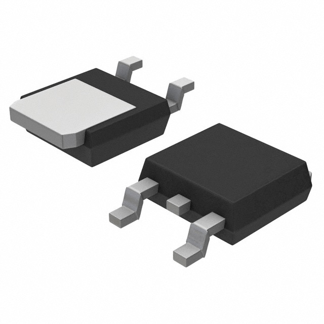
NJVMJD50T4G

Why Choose Us?
Professional Platform
B2B & B2C purchasingDelivery at full speed
1-2 days deliveryWide variety
Original manufacturers365 days guarantee
Responsible quality
.png)


Tech Specifications
NJVMJD50T4G Description
NJVMJD50T4G Description
The NJVMJD50T4G is a high-performance NPN bipolar transistor designed and manufactured by onsemi. This device is engineered to deliver exceptional performance in a variety of applications, thanks to its robust technical specifications and advanced design. With a maximum collector-emitter breakdown voltage of 400V, a maximum collector current of 1A, and a maximum power rating of 1.56W, the NJVMJD50T4G is well-suited for high-power and high-voltage applications.
NJVMJD50T4G Features
-
Technical Specifications: The NJVMJD50T4G boasts a 10MHz transition frequency, making it suitable for high-speed switching applications. Its maximum collector current (Ic) is 1A, and it features a low Vce saturation voltage of 1V at 200mA and 1A. The device is also designed to operate within a wide voltage range, with a maximum collector-emitter breakdown voltage of 400V.
-
Performance Benefits: The NJVMJD50T4G offers a high DC current gain (hFE) of at least 30 at 300mA and 10V, ensuring efficient signal amplification. Its surface-mount packaging allows for compact and efficient integration into various electronic systems.
-
Unique Advantages: This device is REACH unaffected, indicating that it does not contain any substances of very high concern (SVHCs). Additionally, it is RoHS3 compliant, making it suitable for use in environmentally friendly applications.
NJVMJD50T4G Applications
The NJVMJD50T4G is ideal for a wide range of applications, including:
-
Power Amplifiers: Its high power rating and low saturation voltage make it suitable for use in power amplifiers, where high efficiency and low distortion are critical.
-
Switching Applications: The NJVMJD50T4G's high transition frequency and low saturation voltage make it an excellent choice for high-speed switching applications, such as in motor control and power management systems.
-
Signal Amplification: Its high DC current gain and low noise characteristics make it well-suited for use in signal amplification circuits, such as in audio equipment and communication systems.
Conclusion of NJVMJD50T4G
In conclusion, the NJVMJD50T4G is a versatile and high-performance NPN bipolar transistor that offers a unique combination of technical specifications, performance benefits, and environmental compliance. Its wide range of applications, from power amplifiers to switching applications, makes it an ideal choice for engineers looking to design high-performance electronic systems. With its robust performance and advanced features, the NJVMJD50T4G is poised to deliver exceptional results in a variety of applications.
FAQ
| Quantity | Unit Price | Ext. Price |
|---|---|---|
| 1+ | $1.91657 | $1.92 |
| 10+ | $1.64400 | $16.44 |
| 30+ | $1.47428 | $44.23 |
Not available to buy online? Want the lower wholesale price? Please Send RFQ to get best price, we will respond immediately


.png?x-oss-process=image/format,webp/resize,h_32)


