

onsemi
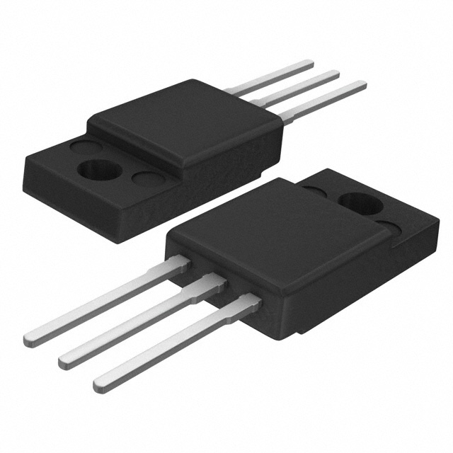
NTPF110N65S3HF
Single FETs, MOSFETs

Not available to buy online? Want the lower wholesale price? Please Send RFQ to get best price, we will respond immediately


.png?x-oss-process=image/format,webp/resize,p_30)


NTPF110N65S3HF Description
NTPF110N65S3HF Description
The NTPF110N65S3HF from onsemi is a high-performance N-channel MOSFET designed for demanding power management applications. With a 650V drain-to-source voltage (Vdss) and 30A continuous drain current (Id), it delivers robust performance in high-voltage circuits. Part of the SuperFET® III FRFET® series, this device leverages advanced Metal Oxide Semiconductor (MOS) technology to achieve low conduction losses and high switching efficiency. Its through-hole TO220FP package ensures reliable thermal management, supporting a maximum power dissipation of 240W (Tc).
NTPF110N65S3HF Features
- Low On-Resistance: 110mΩ (max) at 15A, 10V, minimizing power losses and improving efficiency.
- Fast Switching: Optimized gate charge (Qg) of 62nC @ 10V and input capacitance (Ciss) of 2635pF @ 400V enable high-frequency operation.
- High Voltage Tolerance: Vdss of 650V and Vgs(max) of ±30V ensure durability in harsh environments.
- Thermal Efficiency: TO220FP package enhances heat dissipation, critical for high-power applications.
- Compliance: ROHS3 and REACH compliant, meeting global environmental standards.
NTPF110N65S3HF Applications
This MOSFET is ideal for:
- Switched-Mode Power Supplies (SMPS): High-voltage input stages and PFC circuits.
- Motor Drives: Efficient control in industrial and automotive systems.
- Renewable Energy Systems: Inverters for solar and wind power applications.
- Industrial Power Converters: High-reliability solutions for heavy-duty equipment.
Conclusion of NTPF110N65S3HF
The NTPF110N65S3HF stands out for its high voltage capability, low Rds(on), and robust thermal performance, making it a superior choice for power electronics designers. While marked as "Not For New Designs", its proven reliability in existing applications ensures continued relevance in high-efficiency systems. Its combination of fast switching, low losses, and compliance with environmental standards positions it as a dependable component for industrial and renewable energy applications.
Tech Specifications
NTPF110N65S3HF Documents
Download datasheets and manufacturer documentation for NTPF110N65S3HF
Assembly and Test Qualification 26/Jul/2023 NTPF110N65S3HF NTPF110N65S3HF onsemi RoHS onsemi REACH Material Declaration NTPF110N65S3HF Related Parts


Shopping Guide


.png?x-oss-process=image/format,webp/resize,h_32)


©2025 ERSA Electronics Corporation.