
 German
 Japanese
 Portuguese
 Korea
Korea
 Mexico
 Dutch
Dutch


STMicroelectronics
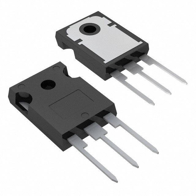
SCTW100N65G2AG

Why Choose Us?
Professional Platform
B2B & B2C purchasingDelivery at full speed
1-2 days deliveryWide variety
Original manufacturers365 days guarantee
Responsible quality
.png)


Tech Specifications
SCTW100N65G2AG Description
STMicroelectronics' SCTW100N65G2AG is a high-power, high-voltage MOSFET transistor designed for use in a variety of applications. Here is a brief description of the model, its features, and potential applications:
Description:
The SCTW100N65G2AG is an N-channel, high-voltage MOSFET transistor from STMicroelectronics. It is designed to operate at high voltages and handle high power levels, making it suitable for use in a variety of applications.
Features:
- N-channel, high-voltage MOSFET transistor
- Designed for high-power applications
- Rated for a maximum drain-source voltage (VDS) of 650V
- Rated for a continuous drain current (ID) of 100A
- Low on-state resistance (RDS(on)) of 0.06 ohms maximum
- High switching speed and low switching losses
- Suitable for use in a wide range of applications
Applications:
The SCTW100N65G2AG is suitable for use in a variety of high-power applications, including:
- Motor control and drive circuits
- Power supply circuits
- Inverter circuits
- Battery management systems
- Renewable energy systems, such as solar power inverters and wind power converters
- Electric vehicle (EV) charging stations
- Industrial control systems
Overall, the SCTW100N65G2AG is a high-power, high-voltage MOSFET transistor that offers excellent performance and reliability in a wide range of applications. Its low on-state resistance and high switching speed make it an ideal choice for use in power electronics circuits where efficiency and performance are critical.
FAQ
Not available to buy online? Want the lower wholesale price? Please Send RFQ to get best price, we will respond immediately


.png?x-oss-process=image/format,webp/resize,h_32)


