
STMicroelectronics
SCTWA50N120
Single FETs, MOSFETs


.png?x-oss-process=image/format,webp/resize,p_30)


SCTWA50N120 Description
SCTWA50N120 Description
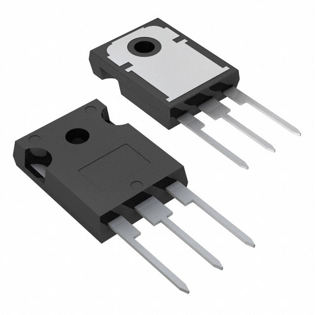
The SCTWA50N120 is a high-performance Silicon Carbide Field-Effect Transistor (SiCFET) from STMicroelectronics, designed for demanding applications that require high voltage and current capabilities. With a drain-to-source voltage (Vdss) of 1200V and a continuous drain current (Id) of 65A at 25°C, this device is suitable for high-power electronics and industrial applications.
SCTWA50N120 Features
- High Voltage and Current Ratings: The SCTWA50N120 boasts a drain-to-source voltage (Vdss) of 1200V and a continuous drain current (Id) of 65A at 25°C, making it ideal for high-power applications.
- Low On-Resistance: With a maximum Rds(on) of 69mΩ at 40A and 20V, this device offers low power dissipation and high efficiency.
- Silicon Carbide Technology: Utilizing SiCFET technology, the SCTWA50N120 provides improved thermal conductivity and faster switching speeds compared to traditional silicon-based MOSFETs.
- Robust Package: The HiP247™ package ensures reliable performance and thermal management in high-power applications.
- Compliance: The SCTWA50N120 is REACH unaffected, RoHS3 compliant, and moisture sensitivity level (MSL) 1, making it suitable for a wide range of applications.
SCTWA50N120 Applications
The SCTWA50N120 is ideal for various high-power applications, including:
- Industrial Motor Drives: Its high voltage and current ratings make it suitable for motor control applications in industrial settings.
- Power Supplies: The low on-resistance and high voltage capabilities make it an excellent choice for power supply designs.
- Renewable Energy Systems: The SCTWA50N120 can be used in solar inverters and wind power systems, where high voltage and current ratings are critical.
- Electric Vehicles: This device is suitable for high-voltage applications in electric vehicles, such as battery management systems and motor controllers.
Conclusion of SCTWA50N120
The SCTWA50N120 from STMicroelectronics is a powerful SiCFET that offers high voltage and current ratings, low on-resistance, and robust performance. Its unique features, such as Silicon Carbide technology and compliance with industry standards, make it an ideal choice for high-power applications in various industries. With its exceptional performance and reliability, the SCTWA50N120 is a valuable addition to any high-power electronics design.
Tech Specifications
SCTWA50N120 Documents
Download datasheets and manufacturer documentation for SCTWA50N120
 SCTWA50N120
 Shopping Guide


.png?x-oss-process=image/format,webp/resize,h_32)


