

STMicroelectronics
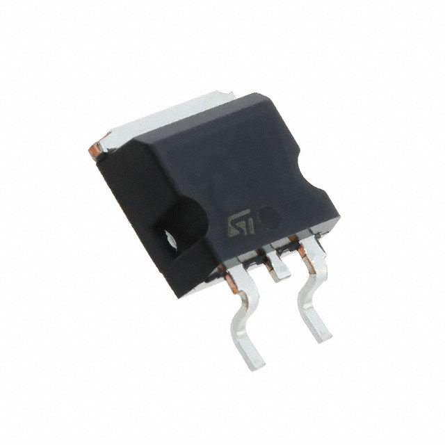
STB45N30M5
Single FETs, MOSFETs

Not available to buy online? Want the lower wholesale price? Please Send RFQ to get best price, we will respond immediately


.png?x-oss-process=image/format,webp/resize,p_30)


STB45N30M5 Description
STB45N30M5 Description
The STB45N30M5 is a high-performance N-channel MOSFET from STMicroelectronics, designed for applications requiring low on-resistance and high efficiency. This MOSFET is part of the MDmesh™ M5 series and is manufactured using advanced technology to ensure superior performance and reliability. With a drain-source voltage rating of 300V and a continuous drain current of 53A at 25°C, the STB45N30M5 is ideal for use in a wide range of power electronics applications.
STB45N30M5 Features
- Low On-Resistance: The STB45N30M5 boasts a typical on-resistance of 0.037 Ohms, which contributes to high efficiency and reduced power loss in power conversion applications.
- High Drain Current: Capable of handling continuous drain currents up to 53A at 25°C, the STB45N30M5 is suitable for high-current applications.
- Robust Voltage Rating: With a drain-source voltage rating of 300V, this MOSFET can be used in high-voltage applications.
- Surface Mount Package: The STB45N30M5 is available in a surface-mount package, making it suitable for use in compact and densely populated PCB designs.
- Compliance with Regulations: The STB45N30M5 is compliant with RoHS3 and REACH standards, ensuring environmental and safety compliance in manufacturing processes.
- Low Gate Charge: The maximum gate charge is 95 nC, which contributes to reduced switching losses and improved efficiency in high-frequency applications.
STB45N30M5 Applications
The STB45N30M5 is ideal for various applications where high efficiency, low on-resistance, and high current handling are required. Some specific use cases include:
- Power Supplies: In switch-mode power supplies (SMPS) and power factor correction (PFC) circuits, the STB45N30M5 can efficiently handle high currents and voltages.
- Motor Drives: The low on-resistance and high current capability make the STB45N30M5 suitable for motor control applications, such as electric vehicles and industrial motor drives.
- Renewable Energy Systems: In solar inverters and wind power systems, the STB45N30M5 can provide efficient power conversion and control.
- Industrial Automation: The STB45N30M5 can be used in industrial automation systems, such as robotics and conveyor systems, where high power and efficiency are critical.
Conclusion of STB45N30M5
The STB45N30M5 from STMicroelectronics is a high-performance N-channel MOSFET that offers a combination of low on-resistance, high current handling, and robust voltage rating. Its compliance with environmental and safety standards, along with its surface-mount package, makes it an ideal choice for a wide range of power electronics applications. The STB45N30M5's unique features and advantages over similar models make it a preferred choice for designers looking for high efficiency and reliability in their power electronics solutions.
Tech Specifications
STB45N30M5 Documents
Download datasheets and manufacturer documentation for STB45N30M5
STB45N30M5 Mult Dev Inner Box Chg 9/Dec/2021 Related Parts


Shopping Guide


.png?x-oss-process=image/format,webp/resize,h_32)


©2025 ERSA Electronics Corporation.