
STMicroelectronics
STP6N60M2
Single FETs, MOSFETs


.png?x-oss-process=image/format,webp/resize,p_30)


STP6N60M2 Description
STP6N60M2 Description
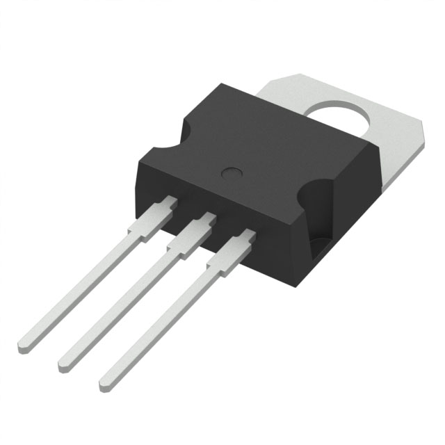
The STP6N60M2 from STMicroelectronics is a 600V N-channel MOSFET designed for high-efficiency power switching applications. Part of the MDmesh™ II Plus series, it combines low on-resistance (1.2Ω @ 10V) with fast switching performance, making it ideal for demanding power conversion tasks. With a continuous drain current (Id) of 4.5A (Tc) and a power dissipation of 60W (Tc), this device is optimized for reliability in high-voltage environments. Its low gate charge (8nC @ 10V) and input capacitance (232pF @ 100V) ensure minimal switching losses, enhancing overall system efficiency. Packaged in a TO-220 through-hole format, it is suitable for industrial, automotive, and consumer applications requiring robust thermal and electrical performance.
STP6N60M2 Features
- High Voltage Rating: 600V Vdss ensures suitability for AC-DC converters, SMPS, and motor drives.
- Low On-Resistance: 1.2Ω @ 10V reduces conduction losses, improving thermal management.
- Fast Switching: Low Qg (8nC) and Ciss (232pF) minimize switching delays and energy losses.
- Robust Construction: MDmesh™ II Plus technology enhances avalanche ruggedness and dv/dt capability.
- Wide Gate Drive Range: ±25V Vgs(max) offers flexibility in gate drive design.
- Compliance: ROHS3, REACH Unaffected, ECCN EAR99, and MSL 1 (Unlimited) ensure environmental and regulatory compatibility.
STP6N60M2 Applications
- Switch-Mode Power Supplies (SMPS): High-voltage input stages and PFC circuits.
- Lighting Systems: Ballasts and LED drivers requiring efficient power handling.
- Motor Control: Inverters and H-bridge configurations for industrial and automotive systems.
- DC-DC Converters: Isolated and non-isolated topologies in telecom and renewable energy systems.
- Consumer Electronics: Power adapters and battery chargers where reliability is critical.
Conclusion of STP6N60M2
The STP6N60M2 stands out as a high-performance 600V MOSFET with low Rds(on), fast switching, and excellent thermal characteristics, making it a preferred choice for power electronics designers. Its MDmesh™ II Plus technology ensures superior efficiency and ruggedness, while its TO-220 package simplifies thermal management in high-power applications. Whether used in SMPS, motor drives, or lighting systems, this MOSFET delivers a balance of cost-effectiveness, reliability, and performance, aligning with modern energy-efficient design requirements.
Tech Specifications
STP6N60M2 Documents
Download datasheets and manufacturer documentation for STP6N60M2
 Product Change Notification 2024-12-04 (PDF) Product Change Notification (PDF) PRODUCT CHANGE NOTIFICATION (PDF) PRODUCT CHANGE NOTIFICATION (PDF)
 Shopping Guide


.png?x-oss-process=image/format,webp/resize,h_32)


