

STMicroelectronics
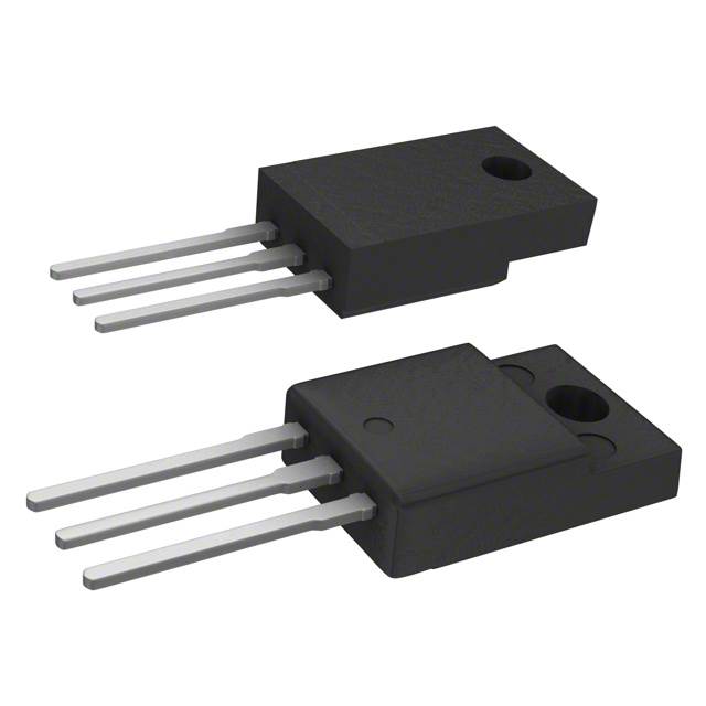
STF6N62K3
Single FETs, MOSFETs

Not available to buy online? Want the lower wholesale price? Please Send RFQ to get best price, we will respond immediately


.png?x-oss-process=image/format,webp/resize,p_30)


STF6N62K3 Description
STF6N62K3 Description
The STF6N62K3 is a high-performance N-Channel MOSFET from STMicroelectronics, designed for applications requiring robust power management and efficient switching. With a drain-to-source voltage (Vdss) of 620V and a continuous drain current (Id) of 5.5A at 25°C, this MOSFET is ideal for high-voltage, high-current applications. Its low on-resistance (Rds On) of 1.28Ohm at 2.8A and 10V, along with a maximum gate-source voltage (Vgs) of ±30V, ensures efficient power dissipation and high-speed switching.
STF6N62K3 Features
- High Voltage and Current Handling: With a Vdss of 620V and Id of 5.5A, the STF6N62K3 can handle high voltage and current loads, making it suitable for power electronics applications.
- Low On-Resistance: The low Rds On of 1.28Ohm at 2.8A and 10V minimizes power losses and improves efficiency.
- Robust Gate Control: The maximum Vgs of ±30V ensures reliable gate control and high-speed switching.
- High-Temperature Operation: The operating temperature range of -55°C to 150°C (TJ) allows the STF6N62K3 to operate in harsh environments.
- Compliance and Environmental: The STF6N62K3 is REACH unaffected, RoHS3 compliant, and has a moisture sensitivity level (MSL) of 1, making it environmentally friendly and suitable for a wide range of applications.
STF6N62K3 Applications
The STF6N62K3 is ideal for various applications where high voltage, high current, and efficient power management are required. Some specific use cases include:
- Power Supplies: In switch-mode power supplies (SMPS) and power factor correction (PFC) circuits, the STF6N62K3 can handle high voltage and current loads while minimizing power losses.
- Motor Controls: For electric vehicle (EV) motor drives and industrial motor control applications, the STF6N62K3 provides efficient switching and high current handling capabilities.
- Renewable Energy Systems: In solar inverters and wind power systems, the STF6N62K3 can manage high voltage and current loads while ensuring efficient power conversion.
Conclusion of STF6N62K3
The STF6N62K3 from STMicroelectronics is a powerful N-Channel MOSFET designed for high-voltage, high-current applications. Its unique combination of high voltage and current handling, low on-resistance, and robust gate control makes it an ideal choice for power electronics, motor controls, and renewable energy systems. With its compliance and environmental certifications, the STF6N62K3 is a reliable and efficient solution for demanding applications in the electronics industry.
Tech Specifications
STF6N62K3 Documents
Download datasheets and manufacturer documentation for STF6N62K3
STx6N62K3 Box Label Chg 28/Jul/2016 STF6N62K3 View All Specifications STx6N62K3 STF6N62K3 Spice Model Marking Layout 10/May/2023 Related Parts


Shopping Guide


.png?x-oss-process=image/format,webp/resize,h_32)


©2025 ERSA Electronics Corporation.