

STMicroelectronics
STL4N10F7
Single FETs, MOSFETs

Not available to buy online? Want the lower wholesale price? Please Send RFQ to get best price, we will respond immediately


- 1+
- $0.74626
- $0.75
- 10+
- $0.64514
- $6.45
- 30+
- $0.58248
- $17.47
- 100+
- $0.51768
- $51.77
- 500+
- $0.48849
- $244.24
- 1000+
- $0.47567
- $475.67

.png?x-oss-process=image/format,webp/resize,p_30)


STL4N10F7 Description
STL4N10F7 Description
The STL4N10F7 is a high-performance N-Channel MOSFET from STMicroelectronics, designed for applications requiring high power dissipation and low on-resistance. With a drain-to-source voltage (Vdss) of 100V and a continuous drain current (Id) of 4.5A at 25°C, this device is ideal for power management and motor control applications. The STL4N10F7 is manufactured using advanced MOSFET technology, ensuring high efficiency and reliability in demanding environments.
STL4N10F7 Features
- High Drain-to-Source Voltage (Vdss): 100V, suitable for high-voltage applications.
- Continuous Drain Current (Id): 4.5A at 25°C, 18A at Tc, providing high current handling capability.
- Low On-Resistance (Rds On): 70mOhm at 2.25A, 10V, reducing power losses and improving efficiency.
- Low Gate Threshold Voltage (Vgs(th)): 4.5V at 250µA, enabling easy gate drive and control.
- High Input Capacitance (Ciss): 408 pF at 50V, minimizing capacitive losses and improving switching performance.
- Low Gate Charge (Qg): 7.8 nC at 10V, reducing switching losses and improving efficiency.
- Robust Power Dissipation: 2.9W (Ta), 50W (Tc), suitable for high-power applications.
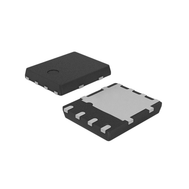
- Surface Mount Technology: PowerFlat™ (3.3x3.3) package,PCB。
- Compliance with Industry Standards: REACH Unaffected, ROHS3 Compliant, and Moisture Sensitivity Level (MSL) 1, ensuring environmental and safety compliance.
STL4N10F7 Applications
The STL4N10F7 is ideal for a wide range of high-power applications, including:
- Power Management: Voltage regulation, power conversion, and distribution in electronic devices.
- Motor Control: High-efficiency motor drivers, particularly in industrial and automotive applications.
- Battery Management Systems: Battery charging and protection circuits in portable devices and electric vehicles.
- Industrial Automation: High-power switching and control in robotic and automation systems.
- Renewable Energy Systems: Power conversion and management in solar and wind energy systems.
Conclusion of STL4N10F7
The STL4N10F7 from STMicroelectronics is a high-performance N-Channel MOSFET, offering a combination of high voltage, low on-resistance, and low gate charge. Its advanced technology, robust power dissipation, and compliance with industry standards make it an ideal choice for demanding high-power applications. With its unique features and advantages, the STL4N10F7 stands out from similar models, providing a reliable and efficient solution for power management and motor control applications.
Tech Specifications
STL4N10F7 Documents
Download datasheets and manufacturer documentation for STL4N10F7
Product Change Notification (PDF) PRODUCT / PROCESS CHANGE INFORMATION (PDF) Related Parts


Shopping Guide


.png?x-oss-process=image/format,webp/resize,h_32)


©2025 ERSA Electronics Corporation.