
 German
 Japanese
 Portuguese
 Korea
Korea
 Mexico
 Dutch
Dutch


STMicroelectronics
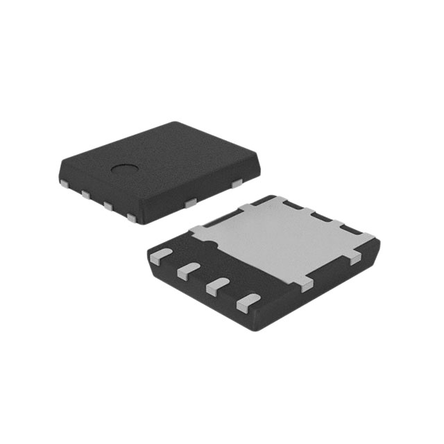
STL6P3LLH6

Why Choose Us?
Professional Platform
B2B & B2C purchasingDelivery at full speed
1-2 days deliveryWide variety
Original manufacturers365 days guarantee
Responsible quality
.png)


Tech Specifications
STL6P3LLH6 Description
STL6P3LLH6 Description
The STL6P3LLH6 from STMicroelectronics is a high-performance P-channel MOSFET designed for power management applications. Part of the STripFET™ H6 series, it features a 30V drain-to-source voltage (Vdss) and a continuous drain current (Id) of 6A at 25°C, making it suitable for medium-power switching tasks. Packaged in a compact PowerFlat™ (3.3x3.3), this surface-mount device offers excellent thermal performance with a maximum power dissipation of 2.9W (Tc). Its low Rds(on) of 30mOhm at 3A, 10V ensures minimal conduction losses, while the ±20V gate-to-source voltage (Vgs) tolerance provides robust gate drive flexibility.
STL6P3LLH6 Features
- Low Gate Charge (Qg): 12nC at 4.5V reduces switching losses, enhancing efficiency in high-frequency applications.
- Fast Switching: Optimized input capacitance (1450pF at 25V) ensures rapid turn-on/off transitions.
- High Reliability: ROHS3 compliant and REACH unaffected, with a moisture sensitivity level (MSL) of 1 (unlimited) for extended shelf life.
- Wide Operating Temperature: 150°C (TJ) rating ensures stable performance in demanding environments.
- Compact Footprint: PowerFlat™ package saves board space while improving thermal dissipation.
STL6P3LLH6 Applications
This MOSFET is ideal for:
- DC-DC Converters: Efficient power conversion in portable devices and industrial systems.
- Load Switching: Low-loss power distribution in battery management systems (BMS).
- Motor Control: Compact driver solutions for automotive and robotics applications.
- Power Supplies: High-efficiency designs for telecom and computing infrastructure.
Conclusion of STL6P3LLH6
The STL6P3LLH6 combines low Rds(on), fast switching, and compact packaging, making it a standout choice for power-efficient designs. Its high current handling, robust thermal performance, and industry-compliant certifications ensure reliability in diverse applications. Engineers seeking a space-saving, high-performance P-channel MOSFET will find this device exceptionally well-suited for modern power electronics challenges.
FAQ
Not available to buy online? Want the lower wholesale price? Please Send RFQ to get best price, we will respond immediately


.png?x-oss-process=image/format,webp/resize,h_32)


