

STMicroelectronics
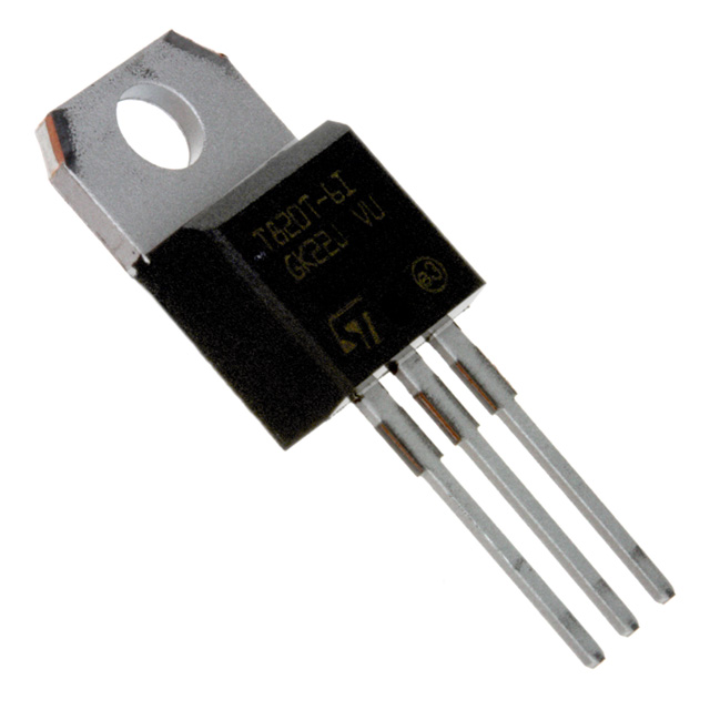
STP200N3LL
Single FETs, MOSFETs

Not available to buy online? Want the lower wholesale price? Please Send RFQ to get best price, we will respond immediately


.png?x-oss-process=image/format,webp/resize,p_30)


STP200N3LL Description
STP200N3LL Description
The STP200N3LL is a high-performance N-Channel MOSFET from STMicroelectronics, designed for applications requiring robust power handling and efficient switching. With a drain-to-source voltage of 30V and a continuous drain current of 120A at 25°C, this device is well-suited for power electronics, motor control, and industrial applications. The STP200N3LL boasts a low on-resistance of 2.4mOhm at 60A and 10V, ensuring minimal power dissipation and high efficiency. Its maximum gate-source voltage is ±20V, providing flexibility in gate drive requirements.
STP200N3LL Features
- Low On-Resistance: The STP200N3LL's low on-resistance of 2.4mOhm at 60A and 10V minimizes power losses and improves efficiency.
- High Drain Current: Capable of handling continuous drain currents up to 120A at 25°C, this MOSFET is ideal for high-power applications.
- Robust Voltage Rating: With a drain-to-source voltage of 30V, the STP200N3LL can be used in a wide range of power electronics applications.
- Low Gate Charge: The maximum gate charge of 53nC at 4.5V reduces switching losses and improves overall efficiency.
- Compliance with Regulations: The STP200N3LL is REACH unaffected and RoHS3 compliant, ensuring environmental and safety standards are met.
- Moisture Sensitivity Level 1: This MOSFET has a moisture sensitivity level of 1, indicating no restrictions on storage or handling.
STP200N3LL Applications
The STP200N3LL is well-suited for a variety of applications where high power handling and efficient switching are required:
- Power Electronics: Due to its high current and voltage ratings, the STP200N3LL is ideal for power supply designs and power conversion circuits.
- Motor Control: The low on-resistance and high current capabilities make this MOSFET suitable for motor drive applications, including electric vehicles and industrial motor control systems.
- Industrial Automation: The STP200N3LL's robust performance characteristics make it a good choice for industrial automation equipment, such as servo drives and robotic systems.
Conclusion of STP200N3LL
The STP200N3LL from STMicroelectronics is a powerful and efficient N-Channel MOSFET, offering a combination of high current handling, low on-resistance, and robust voltage ratings. Its compliance with environmental and safety regulations, along with its moisture sensitivity level, make it a reliable choice for a wide range of applications in power electronics, motor control, and industrial automation. With its unique features and advantages, the STP200N3LL stands out as a high-performance solution in the MOSFET market.
Tech Specifications
STP200N3LL Documents
Download datasheets and manufacturer documentation for STP200N3LL
Product Change Notification (PDF) PRODUCT CHANGE NOTIFICATION (PDF) PRODUCT CHANGE NOTIFICATION (PDF) Related Parts


Shopping Guide


.png?x-oss-process=image/format,webp/resize,h_32)


©2025 ERSA Electronics Corporation.