
 German
 Japanese
 Portuguese
 Korea
Korea
 Mexico
 Dutch
Dutch


STMicroelectronics
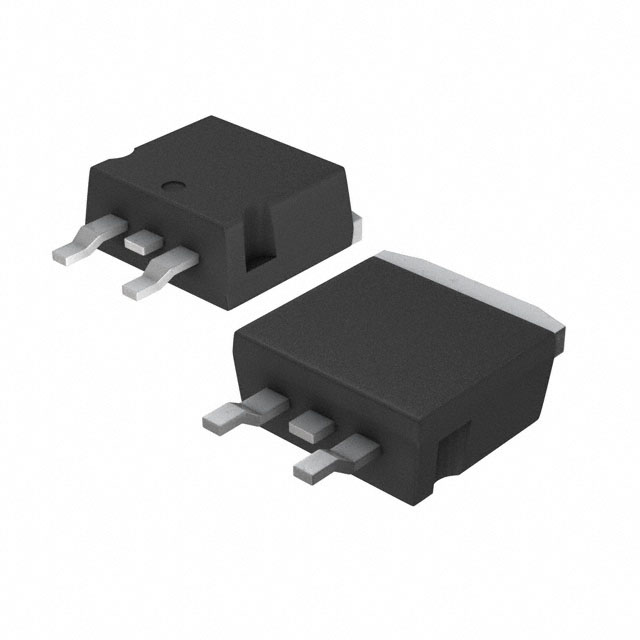
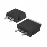
STB9NK90Z
Why Choose Us?
Professional Platform
B2B & B2C purchasingDelivery at full speed
1-2 days deliveryWide variety
Original manufacturers365 days guarantee
Responsible quality
.png)


Tech Specifications
STB9NK90Z Description
STB9NK90Z Description
The STB9NK90Z from STMicroelectronics is a 900V N-channel MOSFET designed for high-voltage switching applications. Part of the SuperMESH™ series, it combines low on-resistance (1.3Ω @ 10V, 3.6A) with high breakdown voltage, making it ideal for power-efficient designs. Packaged in a D2PAK (TO-263) surface-mount form factor, it supports 8A continuous drain current (Id) at 25°C and dissipates up to 160W (Tc). With an input capacitance (Ciss) of 2115pF @ 25V and gate charge (Qg) of 72nC @ 10V, it ensures fast switching performance while minimizing losses.
STB9NK90Z Features
- High Voltage Rating: 900V Vdss for robust performance in demanding applications.
- Low Rds(on): 1.3Ω @ 10V, 3.6A reduces conduction losses, improving efficiency.
- Optimized Gate Drive: 10V drive voltage ensures reliable switching with minimal gate charge (72nC).
- Thermal Efficiency: 160W power dissipation (Tc) and D2PAK package enhance heat management.
- Reliability: ROHS3 compliant, REACH unaffected, and MSL 1 (unlimited) for environmental and handling resilience.
- Wide Vgs Range: ±30V gate-source voltage tolerance for flexible drive circuitry.
STB9NK90Z Applications
- Switched-Mode Power Supplies (SMPS): High-voltage DC-DC converters and offline power supplies.
- Industrial Motor Drives: Efficient switching in inverters and motor control systems.
- Lighting Systems: LED drivers and ballast circuits requiring high-voltage handling.
- Renewable Energy: Solar inverters and energy storage systems benefiting from low Rds(on).
- Automotive Systems: Auxiliary power modules where reliability and efficiency are critical.
Conclusion of STB9NK90Z
The STB9NK90Z stands out for its high-voltage capability, low on-resistance, and thermal performance, making it a superior choice for power electronics. Its SuperMESH™ technology ensures efficiency in high-stress environments, while the D2PAK package offers mechanical and thermal advantages. Ideal for industrial, automotive, and energy applications, this MOSFET delivers a balance of performance, reliability, and cost-effectiveness.
FAQ
Not available to buy online? Want the lower wholesale price? Please Send RFQ to get best price, we will respond immediately


.png?x-oss-process=image/format,webp/resize,h_32)


