
STMicroelectronics
STP2NK100Z
Single FETs, MOSFETs


.png?x-oss-process=image/format,webp/resize,p_30)


STP2NK100Z Description
STP2NK100Z Description
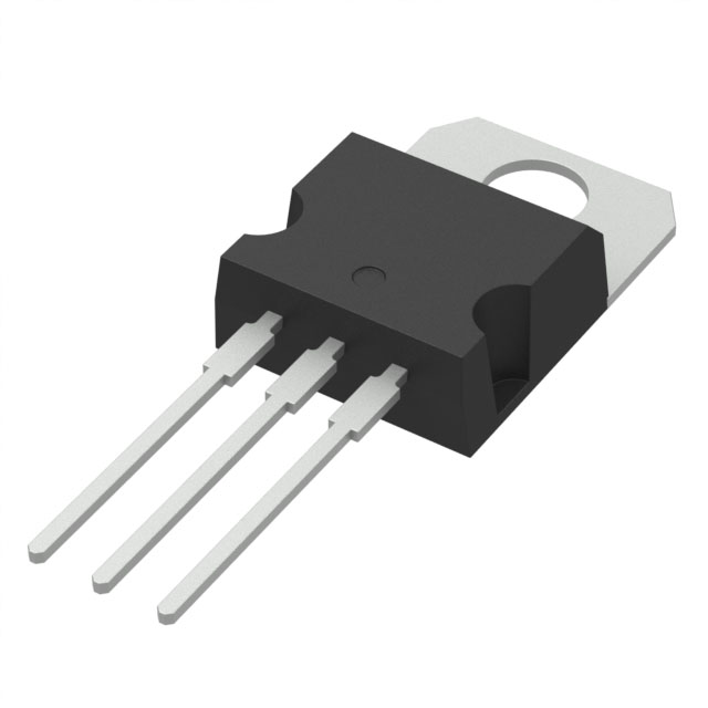
The STP2NK100Z is a high-performance N-Channel MOSFET from STMicroelectronics, designed for applications requiring robust power handling and efficient switching. With a drain-to-source voltage (Vdss) of 1000V and a continuous drain current (Id) of 1.85A at 25°C, this device is well-suited for high-voltage, high-current applications. The STP2NK100Z features a low on-resistance (Rds On) of 8.5Ω at 900mA and 10V, ensuring minimal power dissipation and high efficiency. Its SuperMESH™ technology provides excellent thermal performance and reliability.
STP2NK100Z Features
- High Voltage Rating: 1000V drain-to-source voltage (Vdss) for robust power handling.
- High Current Capacity: 1.85A continuous drain current (Id) at 25°C for high-power applications.
- Low On-Resistance: 8.5Ω Rds On at 900mA and 10V for minimal power dissipation.
- SuperMESH™ Technology: Enhanced thermal performance and reliability.
- Wide Gate Voltage Range: ±30V Vgs (Max) for flexible gate drive compatibility.
- Low Gate Threshold Voltage: 4.5V Vgs(th) (Max) @ 50µA for efficient switching.
- Low Input Capacitance: 499pF Ciss (Max) @ 25V for fast switching and reduced parasitic effects.
- Low Gate Charge: 16nC Qg (Max) @ 10V for reduced switching losses.
- RoHS3 Compliance: Environmentally friendly and suitable for green electronics.
- REACH Unaffected: Compliant with European chemical regulations.
- Moisture Sensitivity Level 1: Unlimited storage time in a dry environment.
STP2NK100Z Applications
The STP2NK100Z is ideal for a variety of high-voltage, high-current applications, including:
- Power Supplies: High-efficiency switching in power supply designs.
- Motor Controls: Reliable operation in motor drive circuits.
- Industrial Automation: Durable performance in harsh industrial environments.
- Automotive Electronics: Reliable operation in high-voltage automotive applications.
- RF Power Amplifiers: Efficient switching in high-power RF amplifiers.
Conclusion of STP2NK100Z
The STP2NK100Z from STMicroelectronics is a high-performance N-Channel MOSFET designed for demanding high-voltage, high-current applications. Its combination of high voltage rating, low on-resistance, and advanced SuperMESH™ technology make it an excellent choice for power supplies, motor controls, industrial automation, automotive electronics, and RF power amplifiers. With its RoHS3 compliance and REACH unaffected status, the STP2NK100Z is also an environmentally friendly option for green electronics.
Tech Specifications
STP2NK100Z Documents
Download datasheets and manufacturer documentation for STP2NK100Z
 STx2NK100Z
  Box Label Chg 28/Jul/2016
  STP2NK100Z View All Specifications
  STx2NK100Z
 Shopping Guide


.png?x-oss-process=image/format,webp/resize,h_32)


