
 German
 Japanese
 Portuguese
 Korea
Korea
 Mexico
 Dutch
Dutch


STMicroelectronics
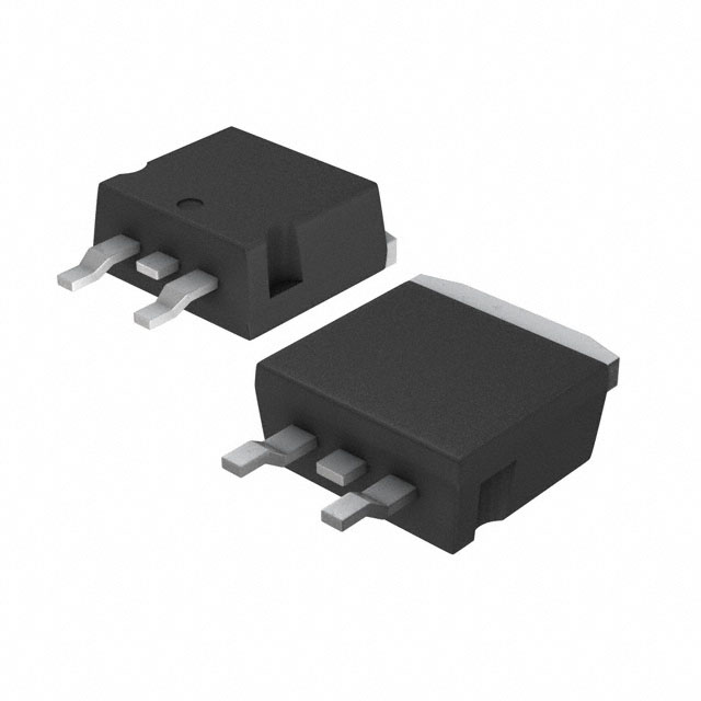
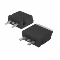
STB9NK80Z

Why Choose Us?
Professional Platform
B2B & B2C purchasingDelivery at full speed
1-2 days deliveryWide variety
Original manufacturers365 days guarantee
Responsible quality
.png)


Tech Specifications
STB9NK80Z Description
STB9NK80Z is a high voltage N-channel power MOSFET from STMicroelectronics. It is designed for high voltage applications and offers excellent electrical characteristics and performance.
Description:
The STB9NK80Z is an N-channel power MOSFET with a voltage rating of 800V and a continuous drain current of 8.0A. It is available in a TO-220 package and features a low on-state resistance (RDS(on)) of 0.08 Ohms maximum at a gate-source voltage (VGS) of 10V.
Features:
- High voltage rating of 800V
- Continuous drain current of 8.0A
- Low on-state resistance (RDS(on)) of 0.08 Ohms maximum at VGS = 10V
- Available in a TO-220 package
- Suitable for high voltage applications
Applications:
The STB9NK80Z is suitable for a wide range of applications that require high voltage and high current handling capabilities. Some of the key applications include:
- Motor control and drive circuits
- Power supplies and converters
- Battery charging and management systems
- Industrial control and automation systems
- High voltage switching and protection circuits
The STB9NK80Z is a reliable and efficient power MOSFET that can be used in a variety of high voltage applications. Its excellent electrical characteristics and performance make it a popular choice for engineers and designers working on power electronics projects.
FAQ
Not available to buy online? Want the lower wholesale price? Please Send RFQ to get best price, we will respond immediately


.png?x-oss-process=image/format,webp/resize,h_32)


