

STMicroelectronics
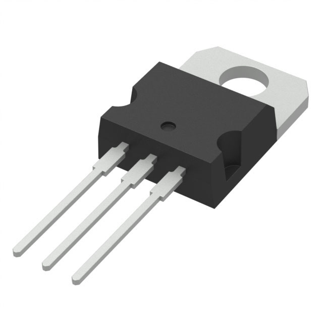
STP23NM50N
Single FETs, MOSFETs

Not available to buy online? Want the lower wholesale price? Please Send RFQ to get best price, we will respond immediately


.png?x-oss-process=image/format,webp/resize,p_30)


STP23NM50N Description
STP23NM50N Description
The STP23NM50N is a high-performance N-channel MOSFET from STMicroelectronics, designed for applications requiring high voltage and current handling capabilities. With a drain-source voltage rating of 500V and a continuous drain current of 17A at 25°C, this device is well-suited for demanding power electronics applications. The STP23NM50N features a low on-resistance of 190mOhm at 8.5A and 10V, ensuring efficient power dissipation and reduced power loss. The device is housed in a TO220-3 package, making it suitable for through-hole mounting in various electronic systems.
STP23NM50N Features
- High Voltage Rating: The STP23NM50N boasts a drain-source voltage rating of 500V, making it ideal for high-voltage applications.
- Low On-Resistance: With an on-resistance of just 190mOhm at 8.5A and 10V, this MOSFET offers efficient power dissipation and reduced power loss.
- High Current Handling: Capable of handling continuous drain currents up to 17A at 25°C, the STP23NM50N is suitable for high-current applications.
- Low Gate Charge: The device features a low gate charge of 45nC at 10V, enabling fast switching and reduced switching losses.
- Robust Temperature Performance: The STP23NM50N operates over a wide temperature range, with a maximum junction temperature of 150°C, making it suitable for harsh environments.
- Compliance: This MOSFET is compliant with the REACH regulation and RoHS3 directive, ensuring environmental and safety compliance.
STP23NM50N Applications
The STP23NM50N is an ideal choice for various high-voltage and high-current applications, including:
- Power Supplies: Due to its high voltage and current ratings, the STP23NM50N is well-suited for power supply designs, particularly in industrial and automotive applications.
- Motor Controls: The device's high current handling capabilities make it suitable for motor control applications, such as in electric vehicles and industrial motor drives.
- Inverters: The STP23NM50N can be used in inverter designs for renewable energy systems, such as solar inverters, due to its ability to handle high voltages and currents.
- Industrial Automation: The robust temperature performance and high voltage rating of this MOSFET make it an excellent choice for industrial automation applications, such as robotic systems and control panels.
Conclusion of STP23NM50N
The STP23NM50N from STMicroelectronics is a high-performance N-channel MOSFET designed for demanding high-voltage and high-current applications. Its combination of low on-resistance, high current handling, and robust temperature performance make it an ideal choice for power supplies, motor controls, inverters, and industrial automation systems. With its compliance to REACH and RoHS3 regulations, the STP23NM50N is not only a high-performance device but also an environmentally responsible choice for electronic design engineers.
Tech Specifications
STP23NM50N Documents
Download datasheets and manufacturer documentation for STP23NM50N
Product Change Notification 2024-12-04 (PDF) TO-220 ECOPACK 2 graded moulding compound assembly capacity expansion - Subcontractor PSI Laguna (Philippines) (PDF) MDmesh II Technology, Power MOSFET Transistors, 8" Wafer size Front-end Capacity Extension - Ang Mo Kio (Singapore) (PDF) Product / Process Change Notification (PDF) Product Change Notification (PDF) PRODUCT CHANGE NOTIFICATION (PDF) Related Parts


Shopping Guide


.png?x-oss-process=image/format,webp/resize,h_32)


©2025 ERSA Electronics Corporation.