
STMicroelectronics
STW20NM50FD
Single FETs, MOSFETs


.png?x-oss-process=image/format,webp/resize,p_30)


STW20NM50FD Description
STW20NM50FD Description
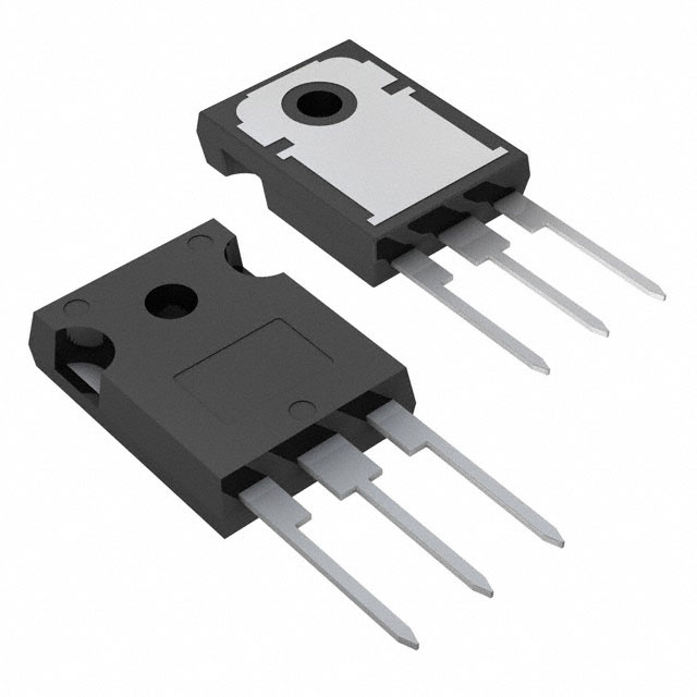
The STW20NM50FD from STMicroelectronics is a high-performance N-channel 500V, 20A power MOSFET designed for demanding switching applications. Packaged in a robust TO-247-3 format, it features FDmesh™ technology, delivering ultra-low on-resistance (250mΩ @ 10A, 10V) and superior switching efficiency. With a gate charge (Qg) of 53nC @ 10V and input capacitance (Ciss) of 1380pF @ 25V, it ensures fast switching speeds while minimizing power losses. The device operates reliably up to 150°C (TJ) and supports a ±30V gate-source voltage (Vgs), making it suitable for high-voltage environments.
STW20NM50FD Features
- High Voltage & Current Rating: 500V Vdss and 20A continuous drain current (Id) for robust power handling.
- Low Rds(on): 250mΩ @ 10V Vgs ensures minimal conduction losses.
- Fast Switching: Optimized Qg (53nC) and Ciss (1380pF) for efficient high-frequency operation.
- Thermal Performance: 214W (Tc) power dissipation and TO-247-3 package for superior heat management.
- Reliability: ROHS3 compliant, REACH unaffected, and MSL 1 (unlimited) for long-term durability.
- Wide Vgs Range: ±30V gate drive tolerance enhances flexibility in circuit design.
STW20NM50FD Applications
- Switched-Mode Power Supplies (SMPS): Ideal for AC-DC converters and high-voltage DC-DC stages.
- Motor Drives & Inverters: Efficiently controls brushless DC (BLDC) motors and industrial inverters.
- Renewable Energy Systems: Suitable for solar inverters and wind power converters due to high voltage tolerance.
- Industrial & Automotive Systems: Used in power factor correction (PFC), UPS systems, and electric vehicle (EV) charging.
Conclusion of STW20NM50FD
The STW20NM50FD stands out as a high-efficiency, high-reliability MOSFET for 500V power switching applications. Its low Rds(on), fast switching, and thermal robustness make it a preferred choice for SMPS, motor drives, and renewable energy systems. With STMicroelectronics' FDmesh™ technology, it outperforms conventional MOSFETs in power density and energy efficiency, ensuring optimal performance in demanding industrial and automotive environments.
Tech Specifications
STW20NM50FD Documents
Download datasheets and manufacturer documentation for STW20NM50FD
 STW20NM50FD
 Shopping Guide


.png?x-oss-process=image/format,webp/resize,h_32)


