
STMicroelectronics
STW55NM60ND
Single FETs, MOSFETs


.png?x-oss-process=image/format,webp/resize,p_30)


STW55NM60ND Description
STW55NM60ND Description
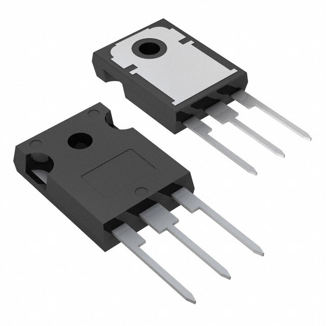
The STW55NM60ND from STMicroelectronics is a high-performance N-channel MOSFET designed for demanding power applications. With a 600V drain-to-source voltage (Vdss) and 51A continuous drain current (Id), it offers robust performance in high-voltage, high-current environments. This device is part of the FDmesh™ II series, leveraging advanced Metal Oxide Semiconductor (MOSFET) technology to deliver low conduction losses and high switching efficiency. Its 60mΩ maximum on-resistance (Rds On) at 10V gate drive ensures minimal power dissipation, making it ideal for energy-efficient designs. Although marked as Obsolete, it remains a reliable choice for legacy systems requiring high-voltage switching.
STW55NM60ND Features
- High Voltage & Current Handling: 600V Vdss and 51A Id for robust power management.
- Low On-Resistance: 60mΩ @ 10V Vgs reduces conduction losses, improving efficiency.
- Fast Switching: Gate charge (Qg) of 190nC @ 10V ensures quick transitions, suitable for high-frequency applications.
- Thermal Performance: 350W power dissipation (Tc) and 150°C max junction temperature (TJ) for reliable operation under thermal stress.
- Compliance & Packaging: ROHS3 compliant, REACH unaffected, and available in a TO-247-3 through-hole package for easy mounting.
- Drive Voltage Flexibility: ±25V Vgs (max) allows compatibility with various gate drivers.
STW55NM60ND Applications
This MOSFET excels in high-power switching applications, including:
- Switch-Mode Power Supplies (SMPS): Efficient power conversion in industrial and telecom systems.
- Motor Drives & Inverters: High-current handling for electric vehicles and industrial motor control.
- Uninterruptible Power Supplies (UPS): Reliable performance in backup power systems.
- Renewable Energy Systems: Solar inverters and wind power converters benefit from its high-voltage capability.
- Welding Equipment: Robust operation in high-power welding machines.
Conclusion of STW55NM60ND
The STW55NM60ND is a high-voltage, high-current MOSFET optimized for efficiency and reliability in power electronics. Its low Rds On, fast switching, and thermal resilience make it suitable for industrial, automotive, and renewable energy applications. While obsolete, its FDmesh™ II technology ensures superior performance in legacy designs requiring durable power switching solutions. Engineers seeking a balance of voltage endurance, current capacity, and thermal management will find this MOSFET a dependable choice.
Tech Specifications
STW55NM60ND Documents
Download datasheets and manufacturer documentation for STW55NM60ND
 Mult Dev Assembly Chg 18/Oct/2019
  STB11NK40Z View All Specifications
  Mult Dev EOL 17/Oct/2018
 Shopping Guide


.png?x-oss-process=image/format,webp/resize,h_32)


