
STMicroelectronics
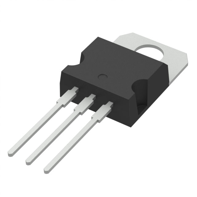
STP11NM60ND
Single FETs, MOSFETs


.png?x-oss-process=image/format,webp/resize,p_30)


STP11NM60ND Description
STP11NM60ND Description
The STP11NM60ND is a high-performance N-Channel MOSFET from STMicroelectronics, designed for applications requiring robust power handling and efficient switching. This MOSFET is part of the FDmesh™ II series, known for its excellent performance and reliability. With a drain-to-source voltage rating of 600V and a continuous drain current of 10A at 25°C, the STP11NM60ND is capable of handling demanding power electronic applications.
STP11NM60ND Features
- 600V Drain-to-Source Voltage (Vdss): Ensures the device can handle high voltage applications without risk of breakdown.
- 10A Continuous Drain Current (Id) @ 25°C: Provides ample current capacity for power electronics applications.
- 450mOhm Rds On (Max) @ 5A, 10V: Offers low on-resistance for efficient power dissipation.
- 5V Vgs(th) (Max) @ 250µA: Facilitates easy gate drive and control.
- 30 nC Gate Charge (Qg) (Max) @ 10V: Minimizes switching losses, contributing to higher efficiency.
- 850 pF Input Capacitance (Ciss) (Max) @ 50 V: Reduces parasitic effects and improves high-frequency performance.
- 90W Power Dissipation (Max): Allows for operation in high-power applications.
- Through Hole Mounting Type: Facilitates easy integration into existing designs.
- ROHS3 Compliance: Ensures environmental sustainability and regulatory compliance.
- Moisture Sensitivity Level (MSL) 1: Indicates unlimited storage time before baking is required, simplifying logistics.
STP11NM60ND Applications
The STP11NM60ND is ideal for a variety of applications where high voltage and current handling are required, such as:
- Power Supplies: Due to its high voltage and current ratings, it is suitable for power supply designs.
- Industrial Controls: The robustness of the STP11NM60ND makes it a good fit for industrial control systems.
- Automotive Electronics: The device's ability to handle high temperatures and voltages makes it suitable for automotive applications.
- Renewable Energy Systems: Its high power dissipation capability is beneficial in solar inverters and wind power systems.
Conclusion of STP11NM60ND
The STP11NM60ND stands out with its combination of high voltage and current ratings, low on-resistance, and compliance with environmental regulations. Its unique features, such as low gate charge and input capacitance, make it an excellent choice for applications demanding high efficiency and performance. The STP11NM60ND's versatility and reliability make it a preferred choice in the electronics industry for high-power applications.
Tech Specifications
STP11NM60ND Documents
Download datasheets and manufacturer documentation for STP11NM60ND
 STx11NM60ND
  STB11NK40Z View All Specifications
  STx11NM60ND
 Shopping Guide


.png?x-oss-process=image/format,webp/resize,h_32)


