

Texas Instruments
CDCLVC1112PW
Clock Buffers, Drivers ICs

Not available to buy online? Want the lower wholesale price? Please Send RFQ to get best price, we will respond immediately


.png?x-oss-process=image/format,webp/resize,p_30)


CDCLVC1112PW Description
CDCLVC1112PW Description
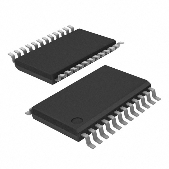
The CDCLVC1112PW is a high-performance clock buffer designed by Texas Instruments, featuring a 1:12 fanout ratio and a maximum operating frequency of 250 MHz. This device is ideal for applications requiring efficient clock distribution with minimal skew and jitter. The CDCLVC1112PW is housed in a 24-TSSOP package, making it suitable for surface-mount applications. It operates within a supply voltage range of 2.3V to 3.6V and supports LVCMOS input and output levels. With its robust design and compliance with industry standards such as REACH and RoHS3, the CDCLVC1112PW ensures reliability and environmental sustainability.
CDCLVC1112PW Features
- High Fanout Ratio: The 1:12 fanout ratio allows for efficient distribution of clock signals to multiple destinations, reducing the need for additional buffering stages.
- Wide Operating Frequency Range: With a maximum operating frequency of 250 MHz, the CDCLVC1112PW can handle high-speed clock signals, making it suitable for demanding applications.
- LVCMOS Compatibility: The device supports LVCMOS input and output levels, ensuring compatibility with a wide range of digital systems.
- Surface-Mount Packaging: The 24-TSSOP package is designed for surface-mount technology, facilitating easy integration into modern PCB designs.
- Wide Supply Voltage Range: The CDCLVC1112PW operates within a supply voltage range of 2.3V to 3.6V, providing flexibility in power supply requirements.
- Environmental Compliance: The device is REACH unaffected and RoHS3 compliant, ensuring it meets stringent environmental standards.
- Moisture Sensitivity Level: With an MSL of 1 (Unlimited), the CDCLVC1112PW is suitable for storage and handling in various environmental conditions.
CDCLVC1112PW Applications
The CDCLVC1112PW is well-suited for a variety of applications where reliable clock distribution is critical. Some specific use cases include:
- Telecommunications: In base stations and network equipment, the CDCLVC1112PW can distribute clock signals to multiple components, ensuring synchronized operation.
- Computing: In servers and high-performance computing systems, the device can provide stable clock signals to various processing units.
- Industrial Automation: For control systems and robotic applications, the CDCLVC1112PW ensures precise timing and synchronization.
- Consumer Electronics: In devices such as gaming consoles and high-definition televisions, the buffer can distribute clock signals to multiple subsystems.
Conclusion of CDCLVC1112PW
The CDCLVC1112PW from Texas Instruments is a versatile and reliable clock buffer that offers significant advantages in clock distribution. Its high fanout ratio, wide operating frequency range, and LVCMOS compatibility make it an ideal choice for a variety of applications. The device's surface-mount packaging, wide supply voltage range, and environmental compliance further enhance its suitability for modern electronic systems. Whether used in telecommunications, computing, industrial automation, or consumer electronics, the CDCLVC1112PW ensures efficient and reliable clock signal distribution, making it a valuable component in any high-performance system.
Tech Specifications
CDCLVC1112PW Documents
Download datasheets and manufacturer documentation for CDCLVC1112PW
Mechanical Outline Drawing Add Cu as Alternative Bond Wire Metal for Select Devices (PDF) Product Change Notification (PDF) CDCLVC1112PW Symbol & Footprint by SnapMagic Clock & Timing Solutions (Rev. C) How to Apply 1.8-V Signals to 3.3-V CDCLVC11xx Fanout Clock Buffer Related Parts


Shopping Guide


.png?x-oss-process=image/format,webp/resize,h_32)


©2025 ERSA Electronics Corporation.