

Texas Instruments
SN74AUP2G07DSFR
Buffers, Drivers, Receivers, Transceivers

Not available to buy online? Want the lower wholesale price? Please Send RFQ to get best price, we will respond immediately


.png?x-oss-process=image/format,webp/resize,p_30)


SN74AUP2G07DSFR Description
SN74AUP2G07DSFR Description
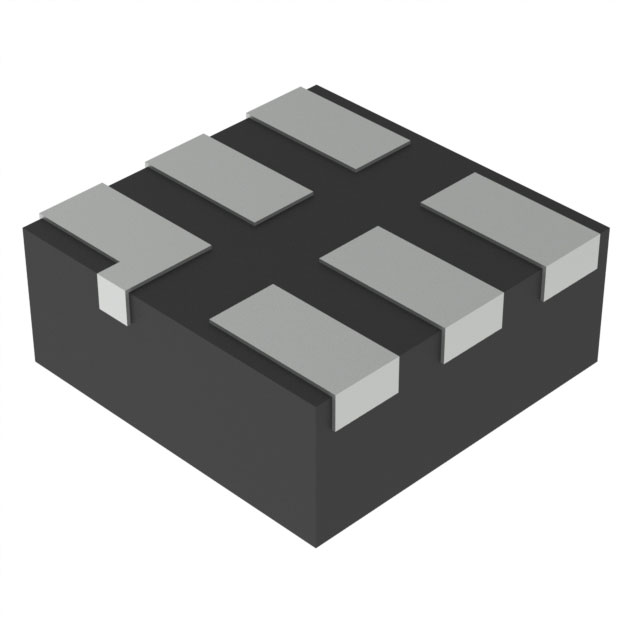
The SN74AUP2G07DSFR is a high-performance, dual non-inverting buffer designed by Texas Instruments. This logic IC chip is part of the 74AUP series, known for its robustness and versatility in various electronic applications. The SN74AUP2G07DSFR features two independent non-inverting buffers, each capable of handling one bit of data. It operates within a wide supply voltage range of 0.8V to 3.6V, making it suitable for a variety of power requirements. The device is designed with an open-drain output type, allowing for flexible interfacing with other electronic components.
SN74AUP2G07DSFR Features
- Number of Bits per Element: 1 bit per buffer element, ensuring precise control and signal integrity.
- Output Type: Open Drain, which provides flexibility in circuit design and compatibility with different voltage levels.
- Supply Voltage Range: 0.8V to 3.6V, offering broad compatibility with various power supply systems.
- Mounting Type: Surface Mount, ideal for compact and high-density PCB designs.
- Product Status: Active, ensuring continued availability and support from Texas Instruments.
- Series: 74AUP, a series renowned for its reliability and performance in logic IC applications.
- Package: Tape & Reel (TR), facilitating efficient handling and assembly in manufacturing processes.
- Moisture Sensitivity Level (MSL): Level 1 (Unlimited), indicating high resistance to moisture and suitability for various environmental conditions.
- Compliance: ROHS3 Compliant and REACH Unaffected, ensuring environmental safety and regulatory compliance.
SN74AUP2G07DSFR Applications
The SN74AUP2G07DSFR is ideal for applications requiring non-inverting buffering of digital signals. Its wide voltage range and open-drain output make it suitable for interfacing between different digital systems. Some specific use cases include:
- Digital Signal Processing: Enhancing signal integrity and buffering in digital signal processing circuits.
- Microcontroller Interfaces: Providing stable buffering between microcontrollers and peripheral devices.
- Communication Systems: Ensuring reliable signal transmission in low-voltage communication protocols.
- Industrial Automation: Utilized in control systems where precise signal buffering is critical.
Conclusion of SN74AUP2G07DSFR
The SN74AUP2G07DSFR from Texas Instruments stands out as a versatile and reliable dual non-inverting buffer. Its wide supply voltage range, open-drain output, and surface-mount design make it suitable for a variety of applications, from digital signal processing to industrial automation. The device's compliance with environmental standards and its active product status ensure long-term availability and support. For engineers and designers seeking a robust and flexible buffering solution, the SN74AUP2G07DSFR is an excellent choice.
Tech Specifications
SN74AUP2G07DSFR Documents
Download datasheets and manufacturer documentation for SN74AUP2G07DSFR
Assembly/Test Site Addition 16/Jul/2014 SN74AUP2G07 SN74AUP2G07 SN74AUP2G07 17/Dec/2021 Related Parts


Shopping Guide


.png?x-oss-process=image/format,webp/resize,h_32)


©2025 ERSA Electronics Corporation.