

Not available to buy online? Want the lower wholesale price? Please Send RFQ to get best price, we will respond immediately


- 1+
- $36.12895
- $36.13
- 3+
- $33.12994
- $99.39
- 30+
- $31.63788
- $949.14

.png?x-oss-process=image/format,webp/resize,p_30)


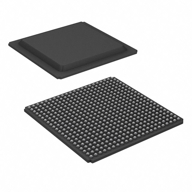
XC7A100T-2FGG484I Description
The XC7A100T-2FGG484I is a high-performance Field Programmable Gate Array (FPGA) device manufactured by AMD (formerly Xilinx). It belongs to the Artix-7 series, which is designed for a wide range of applications requiring moderate gate density and high performance.
Description:
The XC7A100T-2FGG484I is a 2FGG484 package with a T (industrial temperature range) grade. It features a 28-nm manufacturing process and is designed for use in a variety of applications, including but not limited to communications, industrial control, automotive, and consumer electronics.
Features:
- Moderate Gate Density: The XC7A100T-2FGG484I provides a suitable balance between gate density and performance, making it suitable for a wide range of applications.
- Industrial Temperature Range: The 'T' grade in the model number indicates that the device is designed to operate in industrial temperature ranges, typically between -40°C and +85°C or -40°C and +105°C, depending on the specific package.
- High Performance: The device offers high-speed performance, with a maximum operating frequency of up to 1 GHz, depending on the design and application.
- Low Power Consumption: The 28-nm manufacturing process allows for lower power consumption compared to older FPGA technologies.
- Integrated Block RAM (BRAM): The device includes a significant amount of Block RAM, which can be used for data storage and high-speed access.
- Digital Signal Processing (DSP) Blocks: The XC7A100T-2FGG484I features DSP blocks that can be used for high-speed mathematical operations and signal processing tasks.
- High-Bandwidth Memory (HBM) Interface: The device supports high-bandwidth memory interfaces, allowing for efficient data transfer between the FPGA and external memory.
- I/O Capabilities: The FPGA offers a wide range of I/O options, including high-speed transceivers, making it suitable for various communication protocols and interfaces.
Applications:
- Communications: The XC7A100T-2FGG484I can be used in communication systems, such as 5G base stations, optical transport networks, and data center interconnects.
- Industrial Control: The device can be utilized in industrial automation and control systems, where real-time processing and reliable operation are critical.
- Automotive: The XC7A100T-2FGG484I can be employed in automotive applications, such as advanced driver assistance systems (ADAS), in-vehicle networking, and infotainment systems.
- Consumer Electronics: The FPGA can be used in consumer electronics, such as smart home devices, gaming consoles, and high-definition video processing systems.
- Aerospace and Defense: The device can be employed in aerospace and defense applications, where high reliability and performance are essential.
In summary, the AMD XC7A100T-2FGG484I is a versatile, high-performance FPGA device suitable for a wide range of applications, from communications and industrial control to automotive and consumer electronics. Its moderate gate density, industrial temperature range, and advanced features make it a popular choice for designers looking for a balance between performance and complexity.
Tech Specifications
XC7A100T-2FGG484I Documents
Download datasheets and manufacturer documentation for XC7A100T-2FGG484I
 XC7A100T/200T Errata 7 Series FPGA Overview Artix-7 FPGAs Datasheet Artix-7 FPGAs Brief Xilinx REACH211 Cert Xiliinx RoHS Cert
 Related Parts


Relevant Search
Shopping Guide


.png?x-oss-process=image/format,webp/resize,h_32)


©2025 ERSA Electronics Corporation.