
 German
 Japanese
 Portuguese
 Korea
Korea
 Mexico
 Dutch
Dutch


STMicroelectronics
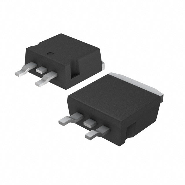
STB55NF06T4
Why Choose Us?
Professional Platform
B2B & B2C purchasingDelivery at full speed
1-2 days deliveryWide variety
Original manufacturers365 days guarantee
Responsible quality
.png)


Tech Specifications
STB55NF06T4 Description
STB55NF06T4 Description
The STB55NF06T4 is a high-performance N-Channel MOSFET from STMicroelectronics, designed for applications requiring high efficiency and robustness. This device features a drain-to-source voltage of 60V, continuous drain current of 50A at 25°C, and a maximum power dissipation of 110W. With a low on-resistance of 18mOhm at 27.5A and 10V gate-source voltage, the STB55NF06T4 offers superior performance in power management and motor control applications.
STB55NF06T4 Features
- Technology: MOSFET (Metal Oxide) - Provides excellent electrical characteristics and reliability.
- Series: STripFET™ II - STMicroelectronics' advanced series for high-efficiency power management.
- Input Capacitance (Ciss): 1300 pF @ 25V - Minimizes input capacitance for faster switching and reduced power loss.
- Gate Charge (Qg): 60 nC @ 10V - Reduces switching losses and improves efficiency.
- Vgs (Max): ±20V - Offers wide gate voltage range for compatibility with various gate drivers.
- Rds On (Max): 18mOhm @ 27.5A, 10V - Ensures low on-resistance for minimal power dissipation.
- Vgs(th) (Max): 4V @ 250µA - Provides a low threshold voltage for easy gate drive.
- Mounting Type: Surface Mount - Facilitates integration into compact and dense PCB layouts.
- Moisture Sensitivity Level (MSL): 1 (Unlimited) - Allows for flexible handling and storage without strict moisture control.
STB55NF06T4 Applications
The STB55NF06T4 is ideal for a variety of applications where high efficiency, low power loss, and robust performance are critical:
- Power Management: In power supply designs, the STB55NF06T4's low on-resistance and high efficiency help reduce power dissipation and improve overall system performance.
- Motor Control: The device's high current capability and fast switching make it suitable for motor drive applications, such as electric vehicles, industrial automation, and robotics.
- Industrial Automation: The STB55NF06T4's robustness and reliability make it a preferred choice for demanding industrial applications, including motor drives, power conversion, and control systems.
Conclusion of STB55NF06T4
The STB55NF06T4 from STMicroelectronics is a high-performance N-Channel MOSFET designed for demanding power management and motor control applications. Its advanced STripFET™ II technology, low on-resistance, and high efficiency make it an ideal choice for applications requiring high performance and reliability. With its wide gate voltage range, low threshold voltage, and surface mount packaging, the STB55NF06T4 offers a versatile solution for a variety of applications in power management, motor control, and industrial automation.
FAQ
| Quantity | Unit Price | Ext. Price |
|---|---|---|
| 1+ | $1.12972 | $1.13 |
| 10+ | $0.94457 | $9.45 |
| 30+ | $0.84343 | $25.30 |
| 100+ | $0.72857 | $72.86 |
| 500+ | $0.67715 | $338.57 |
Not available to buy online? Want the lower wholesale price? Please Send RFQ to get best price, we will respond immediately


.png?x-oss-process=image/format,webp/resize,h_32)


