

STMicroelectronics
STD11N60M6
Single FETs, MOSFETs

Not available to buy online? Want the lower wholesale price? Please Send RFQ to get best price, we will respond immediately


.png?x-oss-process=image/format,webp/resize,p_30)


STD11N60M6 Description
STD11N60M6 Description
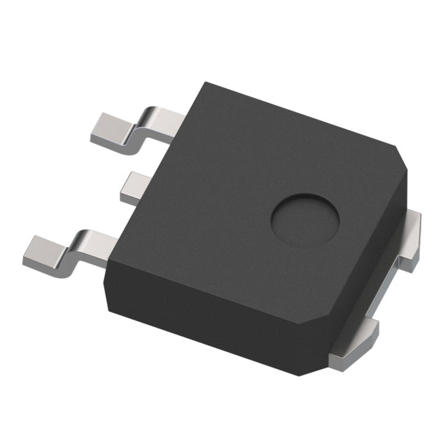
The STD11N60M6 is a high-performance MOSFET (Metal Oxide) from STMicroelectronics, designed for use in a variety of electronic applications. With a drain-to-source voltage (Vdss) of 600V and a power dissipation of up to 90W, this device offers excellent performance and reliability. The STD11N60M6 is currently in active production, ensuring consistent availability and support for your projects.
STD11N60M6 Features
- Input Capacitance (Ciss): The STD11N60M6 boasts a maximum input capacitance of 387 pF at 100V, ensuring fast switching speeds and minimal signal distortion.
- Gate Charge (Qg): With a maximum gate charge of 10.3 nC at 10V, this MOSFET minimizes power loss and heat generation, improving overall efficiency.
- Rds On (Max): The STD11N60M6 offers a low on-resistance of 520mOhm at 4A and 10V, reducing power dissipation and heat generation.
- Vgs(th) (Max): This MOSFET has a maximum threshold voltage of 4.75V at 250µA, ensuring reliable operation across a wide range of input voltages.
- Current - Continuous Drain (Id): The STD11N60M6 can handle continuous drain currents of up to 8A at 25°C, making it suitable for high-current applications.
- Drive Voltage: The maximum drive voltage for this MOSFET is 10V, ensuring compatibility with a wide range of control circuits.
- Mounting Type: The STD11N60M6 is available in a surface-mount package, allowing for easy integration into compact designs.
STD11N60M6 Applications
The STD11N60M6 is ideal for use in various applications, including:
- Power Electronics: Due to its high voltage and current ratings, this MOSFET is well-suited for power electronics applications, such as power supplies and motor control.
- Automotive: The STD11N60M6's robust performance makes it suitable for automotive applications, including electric vehicle (EV) charging systems and power management.
- Industrial Control: This MOSFET's high power dissipation and low on-resistance make it an excellent choice for industrial control systems, such as motor drives and inverters.
Conclusion of STD11N60M6
The STD11N60M6 from STMicroelectronics is a high-performance MOSFET that offers excellent technical specifications and performance benefits. Its unique features, such as low on-resistance, high input capacitance, and robust power dissipation, make it an ideal choice for a wide range of applications, including power electronics, automotive, and industrial control. With its active product status and compliance with various industry standards, the STD11N60M6 is a reliable and efficient solution for your electronic design needs.
Tech Specifications
STD11N60M6 Documents
Download datasheets and manufacturer documentation for STD11N60M6
Product Change Notification (PDF) Related Parts


Shopping Guide


.png?x-oss-process=image/format,webp/resize,h_32)


©2025 ERSA Electronics Corporation.