

STMicroelectronics
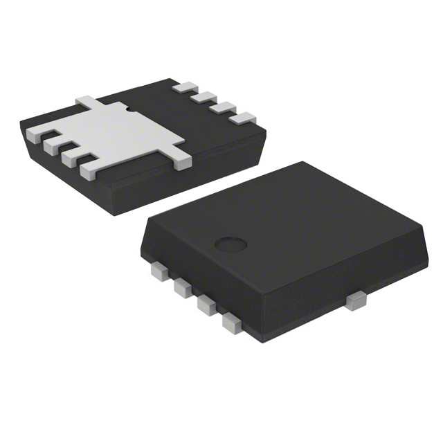
STL8N6F7
Single FETs, MOSFETs

Not available to buy online? Want the lower wholesale price? Please Send RFQ to get best price, we will respond immediately


.png?x-oss-process=image/format,webp/resize,p_30)


STL8N6F7 Description
STL8N6F7 Description
The STL8N6F7 is a high-performance N-Channel MOSFET from STMicroelectronics, designed for power electronics applications. It offers a robust combination of technical specifications and performance benefits, making it an ideal choice for various applications. The device features a maximum drain-source voltage (Vdss) of 60V and a continuous drain current (Id) of 36A at 25°C. With a maximum power dissipation of 3W at ambient temperature and 60W at case temperature, the STL8N6F7 can handle demanding power requirements.
STL8N6F7 Features
- Technology: MOSFET (Metal Oxide) - Provides excellent electrical characteristics and reliability.
- Input Capacitance (Ciss): 450 pF @ 25V - Minimizes input capacitance for faster switching speeds.
- Gate Charge (Qg): 8 nC @ 10V - Reduces switching losses and improves efficiency.
- Rds On (Max): 25mOhm @ 4A, 10V - Offers low on-resistance for minimal power dissipation.
- Vgs(th) (Max): 4V @ 250µA - Ensures reliable turn-on and stable operation.
- Drive Voltage: 10V - Simplifies gate drive requirements.
- Mounting Type: Surface Mount - Facilitates integration into compact designs.
- Package: PowerFlat™ (3.3x3.3) - Delivers high power density in a small footprint.
- REACH Status: REACH Unaffected - Complies with European chemical regulations.
- RoHS Status: ROHS3 Compliant - Meets environmental standards for hazardous substances.
- Moisture Sensitivity Level (MSL): 1 (Unlimited) - Suitable for a wide range of manufacturing processes.
STL8N6F7 Applications
The STL8N6F7 is ideal for various power electronics applications, including:
- Motor Control: Its low on-resistance and high current capability make it suitable for motor drive circuits.
- Power Supplies: The device's high voltage and power dissipation ratings are well-suited for power supply designs.
- Automotive Electronics: The STL8N6F7 can be used in automotive applications, such as electric power steering and battery management systems.
- Industrial Control: Its robust performance characteristics make it suitable for industrial control systems and power conversion applications.
Conclusion of STL8N6F7
The STL8N6F7 is a versatile and high-performance N-Channel MOSFET from STMicroelectronics. Its unique combination of technical specifications, performance benefits, and compliance with environmental standards make it an excellent choice for a wide range of power electronics applications. With its low on-resistance, high current capability, and compact package, the STL8N6F7 delivers reliable performance and efficiency in demanding power electronics designs.
Tech Specifications
STL8N6F7 Documents
Download datasheets and manufacturer documentation for STL8N6F7
Carrier/Cover Tape Supplier 23/Sep/2021 STL8N6F7 Datasheet Related Parts


Shopping Guide


.png?x-oss-process=image/format,webp/resize,h_32)


©2025 ERSA Electronics Corporation.