
 German
 Japanese
 Portuguese
 Korea
Korea
 Mexico
 Dutch
Dutch


STMicroelectronics
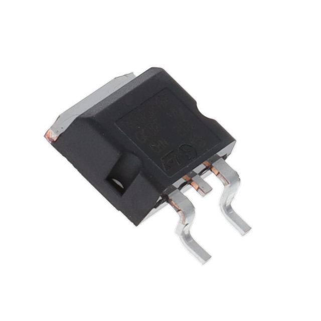
STB26N60M2

Why Choose Us?
Professional Platform
B2B & B2C purchasingDelivery at full speed
1-2 days deliveryWide variety
Original manufacturers365 days guarantee
Responsible quality
.png)


Tech Specifications
STB26N60M2 Description
STB26N60M2 Description
The STB26N60M2 is a high-performance MOSFET N-CHANNEL device manufactured by STMicroelectronics. This single FET is designed to deliver exceptional performance in various applications, thanks to its advanced MOSFET (Metal Oxide) technology. With a drain-to-source voltage (Vdss) of 600V and a continuous drain current (Id) of 20A at 25°C, the STB26N60M2 is capable of handling high power requirements. Its low Rds On of 165mOhm at 10A and 10V ensures efficient power dissipation, with a maximum power dissipation (Pd) of 169W at Tc. The device is mounted on a D2PAK package, making it suitable for surface mount applications.
STB26N60M2 Features
- High Voltage and Current Handling: The STB26N60M2 can handle a drain-to-source voltage of 600V and a continuous drain current of 20A at 25°C, making it ideal for high-power applications.
- Low Rds On: With a maximum Rds On of 165mOhm at 10A and 10V, the STB26N60M2 offers efficient power dissipation and reduced power losses.
- Advanced MOSFET Technology: Utilizing MOSFET (Metal Oxide) technology, the STB26N60M2 provides improved performance and reliability compared to traditional FETs.
- Surface Mount Package: The D2PAK package allows for easy integration into surface mount applications, reducing overall footprint and improving manufacturing efficiency.
- Compliance and Environmental Standards: The STB26N60M2 is compliant with RoHS3 and REACH standards, ensuring environmental responsibility and regulatory compliance.
STB26N60M2 Applications
The STB26N60M2 is ideal for a variety of applications where high voltage and current handling are required. Some specific use cases include:
- Power Supplies: The STB26N60M2 can be used in power supply designs, such as switching power supplies and voltage regulators, where high voltage and current handling are critical.
- Industrial Automation: In industrial automation systems, the STB26N60M2 can be employed in motor control applications, providing efficient power management and control.
- Automotive Applications: The STB26N60M2 is suitable for automotive applications, such as electric vehicle charging systems and power management, where high voltage and current handling are essential.
- Renewable Energy Systems: In renewable energy systems, such as solar inverters and wind turbines, the STB26N60M2 can be used to manage and control high power requirements.
Conclusion of STB26N60M2
The STB26N60M2 is a high-performance MOSFET N-CHANNEL device that offers exceptional voltage and current handling capabilities, making it ideal for a wide range of high-power applications. Its advanced MOSFET technology, low Rds On, and compliance with environmental standards make it a standout choice in the electronics industry. With its unique features and advantages, the STB26N60M2 is a reliable and efficient solution for power management and control in various applications.
FAQ
Not available to buy online? Want the lower wholesale price? Please Send RFQ to get best price, we will respond immediately


.png?x-oss-process=image/format,webp/resize,h_32)


