
 German
 Japanese
 Portuguese
 Korea
Korea
 Mexico
 Dutch
Dutch


STMicroelectronics
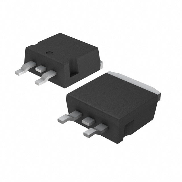
STB75NF75T4

Why Choose Us?
Professional Platform
B2B & B2C purchasingDelivery at full speed
1-2 days deliveryWide variety
Original manufacturers365 days guarantee
Responsible quality
.png)


Tech Specifications
STB75NF75T4 Description
STB75NF75T4 Description
The STB75NF75T4 is a high-performance N-Channel MOSFET from STMicroelectronics, designed for applications requiring robust power handling and efficient switching. This device is part of the STripFET™ II series, known for its superior performance and reliability. With a drain-to-source voltage (Vdss) of 75V and a continuous drain current (Id) of 80A at 25°C, the STB75NF75T4 is capable of handling demanding power electronic applications.
STB75NF75T4 Features
- High Voltage and Current Ratings: The STB75NF75T4 boasts a drain-to-source voltage of 75V and can handle a continuous drain current of 80A at 25°C, making it suitable for high-power applications.
- Low On-Resistance: With a maximum on-resistance (Rds On) of 11mΩ at 40A and 10V, this MOSFET offers efficient power dissipation, reducing power losses and improving overall efficiency.
- Robust Gate Drive: The device has a maximum gate-source voltage (Vgs) of ±20V, ensuring reliable operation across a wide range of gate drive conditions.
- Low Gate Charge: The maximum gate charge (Qg) is 160nC at 10V, contributing to faster switching speeds and lower switching losses.
- Surface Mount Packaging: The D2PAK package allows for easy integration into surface-mount applications, providing a compact and efficient solution for space-constrained designs.
- Compliance and Certifications: The STB75NF75T4 is compliant with RoHS3 and REACH regulations, ensuring environmental and safety standards are met.
STB75NF75T4 Applications
The STB75NF75T4 is ideal for a variety of applications where high power handling and efficient switching are critical:
- Power Supplies: Due to its high voltage and current ratings, the STB75NF75T4 is well-suited for power supply designs, particularly in applications requiring high efficiency and low power losses.
- Motor Controls: The low on-resistance and robust gate drive make this MOSFET an excellent choice for motor control applications, where precise control and high power handling are necessary.
- Automotive Electronics: The STB75NF75T4's ability to handle high voltages and currents, combined with its robustness, makes it suitable for automotive applications, such as electric vehicle chargers and power management systems.
Conclusion of STB75NF75T4
The STB75NF75T4 from STMicroelectronics is a powerful and efficient N-Channel MOSFET, designed to meet the demands of high-power applications. Its combination of high voltage and current ratings, low on-resistance, and compliance with environmental and safety standards make it an excellent choice for power supplies, motor controls, and automotive electronics. The STB75NF75T4's performance benefits and unique features set it apart from similar models, making it a reliable and efficient solution for demanding power electronic applications.
FAQ
Not available to buy online? Want the lower wholesale price? Please Send RFQ to get best price, we will respond immediately


.png?x-oss-process=image/format,webp/resize,h_32)


