
 German
 Japanese
 Portuguese
 Korea
Korea
 Mexico
 Dutch
Dutch


STMicroelectronics
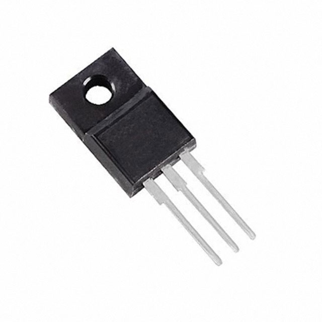
STF33N60DM6

Why Choose Us?
Professional Platform
B2B & B2C purchasingDelivery at full speed
1-2 days deliveryWide variety
Original manufacturers365 days guarantee
Responsible quality
.png)


Tech Specifications
STF33N60DM6 Description
STF33N60DM6 Description
The STF33N60DM6 from STMicroelectronics is a high-performance N-channel 600V MOSFET belonging to the MDmesh™ M6 series, optimized for efficiency and robustness in power electronics. Designed with Metal Oxide Semiconductor (MOSFET) technology, it delivers a continuous drain current (Id) of 25A (Tc) and features an ultra-low on-resistance (Rds(on)) of 128mΩ at 10V gate drive, minimizing conduction losses. Its 600V drain-to-source voltage (Vdss) rating makes it suitable for high-voltage switching applications. Packaged in a TO-220FP through-hole format, it ensures reliable thermal performance with a maximum power dissipation of 35W (Tc).
STF33N60DM6 Features
- Low Gate Charge (Qg): 35nC @ 10V ensures fast switching and reduced drive losses.
- High Voltage Tolerance: 600V Vdss with ±25V Vgs(max) for robust operation in demanding environments.
- Optimized Switching Performance: 1500pF input capacitance (Ciss) balances speed and EMI performance.
- Low Threshold Voltage (Vgs(th)): 4.75V @ 250µA enhances compatibility with low-voltage drivers.
- Reliability Compliance: ROHS3 and REACH compliant, with MSL Not Applicable for easy handling.
- Advanced MDmesh™ M6 Technology: Delivers superior efficiency and thermal stability compared to standard MOSFETs.
STF33N60DM6 Applications
- Switched-Mode Power Supplies (SMPS): High-voltage DC-DC converters and PFC stages.
- Motor Drives: Inverters for industrial and automotive applications requiring high efficiency.
- Lighting Systems: LED drivers and HID ballasts benefiting from low Rds(on).
- Renewable Energy: Solar inverters and energy storage systems leveraging its high voltage rating.
- Industrial Automation: Robust performance in PLCs and high-power switching modules.
Conclusion of STF33N60DM6
The STF33N60DM6 stands out as a high-efficiency, high-voltage MOSFET ideal for power electronics demanding low conduction losses, fast switching, and thermal reliability. Its MDmesh™ M6 technology and optimized gate charge make it superior to conventional MOSFETs in applications like SMPS, motor drives, and renewable energy systems. With STMicroelectronics' proven quality and compliance, this MOSFET is a dependable choice for engineers designing next-generation power solutions.
FAQ
Not available to buy online? Want the lower wholesale price? Please Send RFQ to get best price, we will respond immediately


.png?x-oss-process=image/format,webp/resize,h_32)


