
 German
 Japanese
 Portuguese
 Korea
Korea
 Mexico
 Dutch
Dutch


STMicroelectronics
STF11N65M5

Why Choose Us?
Professional Platform
B2B & B2C purchasingDelivery at full speed
1-2 days deliveryWide variety
Original manufacturers365 days guarantee
Responsible quality
.png)


Tech Specifications
STF11N65M5 Description
STF11N65M5 Description
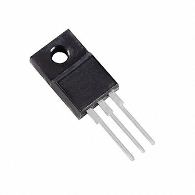
The STF11N65M5 is a high-performance N-Channel MOSFET from STMicroelectronics, designed for a wide range of applications in the electronics industry. This MOSFET is built using advanced Metal Oxide technology, ensuring high efficiency and reliability. With a maximum drain-source voltage (Vdss) of 650V and a continuous drain current (Id) of 9A at 25°C, the STF11N65M5 is capable of handling high voltage and current loads. Its low on-resistance (Rds On) of 480mOhm at 4.5A and 10V ensures minimal power loss and high efficiency in operation. The device is housed in a TO220FP package, making it suitable for through-hole mounting in various electronic systems.
STF11N65M5 Features
- High Voltage and Current Handling: With a Vdss of 650V and Id of 9A, the STF11N65M5 can handle high voltage and current loads, making it ideal for applications requiring high power management.
- Low On-Resistance: The low Rds On of 480mOhm at 4.5A and 10V ensures minimal power loss and high efficiency in operation.
- Advanced Metal Oxide Technology: Built using advanced Metal Oxide technology, the STF11N65M5 offers high efficiency, reliability, and performance.
- Wide Operating Temperature Range: The device can operate at temperatures up to 150°C (TJ), making it suitable for applications with high thermal demands.
- RoHS3 Compliance: The STF11N65M5 is compliant with the RoHS3 directive, ensuring environmental friendliness and adherence to global regulations.
- REACH Unaffected Status: The device is not affected by the REACH regulation, ensuring uninterrupted supply and availability.
STF11N65M5 Applications
The STF11N65M5 is ideal for a variety of applications in the electronics industry, including:
- Power Management: Due to its high voltage and current handling capabilities, the STF11N65M5 is suitable for power management applications in various electronic systems.
- Industrial Control: The device's high performance and reliability make it ideal for industrial control applications, such as motor control and power conversion.
- Automotive Electronics: The STF11N65M5 can be used in automotive electronics for applications like power windows, seat adjustment, and lighting systems.
- Telecommunications: The device's high efficiency and reliability make it suitable for power management in telecommunications equipment, such as base stations and switching systems.
Conclusion of STF11N65M5
The STF11N65M5 is a high-performance N-Channel MOSFET from STMicroelectronics, offering a combination of high voltage and current handling capabilities, low on-resistance, and advanced Metal Oxide technology. Its wide operating temperature range, RoHS3 compliance, and REACH unaffected status make it an ideal choice for a variety of applications in the electronics industry, including power management, industrial control, automotive electronics, and telecommunications. With its unique features and advantages over similar models, the STF11N65M5 is a reliable and efficient solution for high-performance electronic systems.
FAQ
Not available to buy online? Want the lower wholesale price? Please Send RFQ to get best price, we will respond immediately


.png?x-oss-process=image/format,webp/resize,h_32)


