
 German
 Japanese
 Portuguese
 Korea
Korea
 Mexico
 Dutch
Dutch


STMicroelectronics
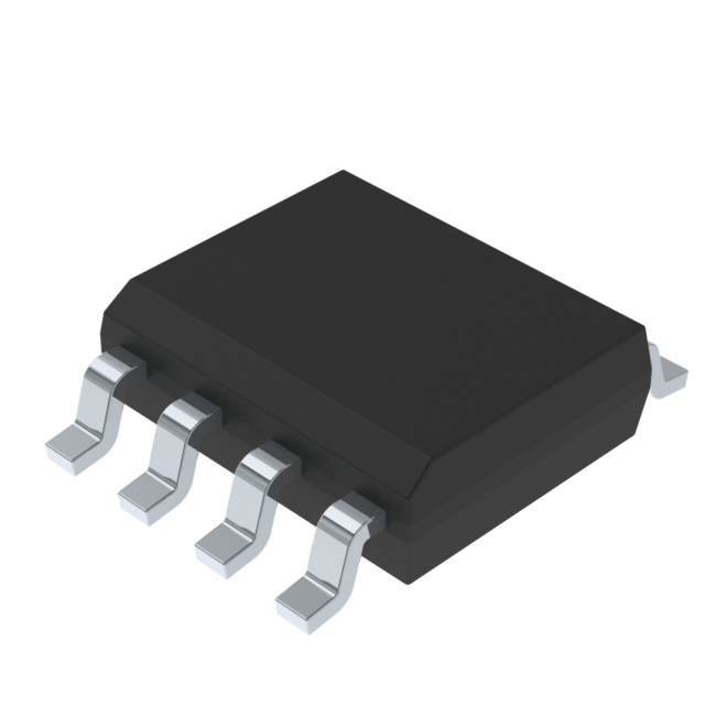
STS6NF20V

Why Choose Us?
Professional Platform
B2B & B2C purchasingDelivery at full speed
1-2 days deliveryWide variety
Original manufacturers365 days guarantee
Responsible quality
.png)


Tech Specifications
STS6NF20V Description
STS6NF20V Description
The STS6NF20V is a high-performance MOSFET N-CH 20V 6A 8SO from STMicroelectronics, designed for applications requiring robust power management and efficient switching. This device is part of the STripFET™ II series, known for its superior performance and reliability. With a maximum drain-source voltage of 20V and a continuous drain current of 6A at 25°C, the STS6NF20V is well-suited for a variety of power electronics applications.
STS6NF20V Features
- Technology: MOSFET (Metal Oxide), leveraging the latest advancements in semiconductor technology for optimal performance.
- Input Capacitance (Ciss): 460 pF @ 15 V, ensuring fast switching and reduced power consumption.
- Gate Charge (Qg): 11.5 nC @ 4.5 V, contributing to high-speed operation and low power loss.
- Rds On (Max): 40mOhm @ 3A, 4.5V, providing low on-resistance for efficient power delivery.
- Vgs(th) (Max): 600mV @ 250µA (Min), allowing for precise control and stable operation.
- Operating Temperature: 150°C (TJ), enabling the device to perform reliably in high-temperature environments.
- Mounting Type: Surface Mount, facilitating easy integration into compact designs.
- REACH Status: REACH Unaffected, ensuring compliance with European chemical regulations.
- RoHS Status: ROHS3 Compliant, adhering to environmental standards for responsible manufacturing.
STS6NF20V Applications
The STS6NF20V is ideal for applications that demand high efficiency and reliability in power management, such as:
- Power Supplies: Due to its low on-resistance and high voltage rating, the STS6NF20V is perfect for power supply designs.
- Motor Controls: Its ability to handle high currents and voltages makes it suitable for motor control applications.
- Automotive Electronics: The device's high-temperature operation and robustness make it a good fit for automotive electronics, where reliability is crucial.
- Industrial Controls: In industrial settings, the STS6NF20V can be used for various control systems that require high power and precision.
Conclusion of STS6NF20V
The STS6NF20V from STMicroelectronics stands out for its superior performance, robust design, and compliance with industry standards. Its unique features, such as low on-resistance and high input capacitance, make it an excellent choice for applications requiring high efficiency and reliability. Whether in power supplies, motor controls, automotive electronics, or industrial controls, the STS6NF20V delivers the performance and reliability that engineers demand.
FAQ
| Quantity | Unit Price | Ext. Price |
|---|---|---|
| 1+ | $0.70457 | $0.70 |
| 10+ | $0.56743 | $5.67 |
| 30+ | $0.49885 | $14.97 |
| 100+ | $0.43028 | $43.03 |
Not available to buy online? Want the lower wholesale price? Please Send RFQ to get best price, we will respond immediately


.png?x-oss-process=image/format,webp/resize,h_32)


