
 German
 Japanese
 Portuguese
 Korea
Korea
 Mexico
 Dutch
Dutch


STMicroelectronics
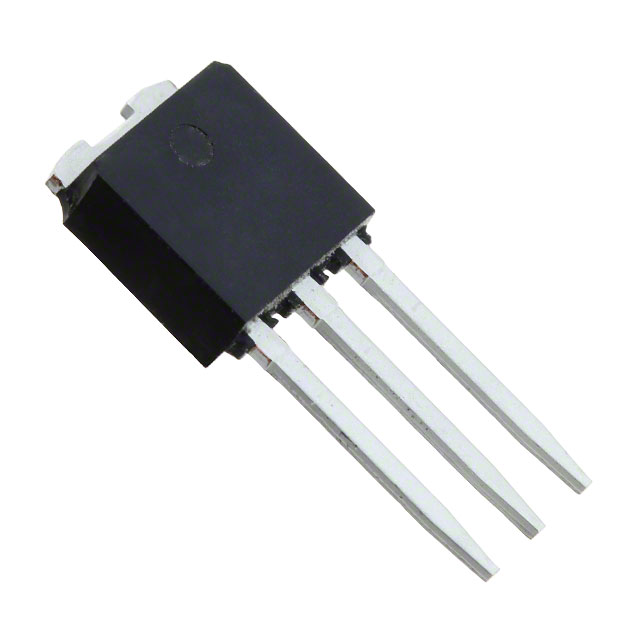
STU2N62K3

Why Choose Us?
Professional Platform
B2B & B2C purchasingDelivery at full speed
1-2 days deliveryWide variety
Original manufacturers365 days guarantee
Responsible quality
.png)


Tech Specifications
STU2N62K3 Description
STU2N62K3 Description
The STU2N62K3 is a high-performance N-channel MOSFET from STMicroelectronics, designed to deliver superior performance in various electronic applications. With a drain-to-source voltage (Vdss) of 620V and a continuous drain current (Id) of 2.2A at 25°C, this device is well-suited for demanding power management tasks. Its low on-resistance (Rds On) of 3.6Ω at 1.1A and 10V VGS ensures high efficiency and minimal power loss. The STU2N62K3 is housed in a through-hole IPAK package, making it ideal for applications requiring high thermal dissipation.
STU2N62K3 Features
- High Voltage and Current Ratings: The STU2N62K3 boasts a drain-to-source voltage (Vdss) of 620V and a continuous drain current (Id) of 2.2A at 25°C, making it suitable for high-voltage applications.
- Low On-Resistance: The device's low on-resistance (Rds On) of 3.6Ω at 1.1A and 10V VGS contributes to high efficiency and minimal power loss.
- Robust Gate Charge Handling: With a maximum gate charge (Qg) of 15nC at 10V VGS, the STU2N62K3 can handle high gate charge requirements without compromising performance.
- Thermal Management: The through-hole IPAK package allows for efficient thermal dissipation, making it suitable for high-power applications.
- Compliance and Environmental: The STU2N62K3 is REACH unaffected, RoHS3 compliant, and has a moisture sensitivity level (MSL) of 1, indicating unlimited storage time before reflow soldering.
STU2N62K3 Applications
The STU2N62K3 is ideal for a wide range of applications, including:
- Power Management: Its high voltage and current ratings make it suitable for power conversion and management in various electronic devices.
- Industrial Automation: The device's robust performance and thermal management capabilities make it ideal for motor control and industrial automation applications.
- Automotive: The STU2N62K3 can be used in automotive applications, such as electric vehicle charging systems and powertrain control.
- Telecommunications: Its high voltage and current ratings make it suitable for power supply and signal processing in telecommunications equipment.
Conclusion of STU2N62K3
The STU2N62K3 from STMicroelectronics is a high-performance N-channel MOSFET that offers superior voltage and current ratings, low on-resistance, and robust gate charge handling. Its through-hole IPAK package ensures efficient thermal dissipation, making it suitable for high-power applications. With its compliance and environmental certifications, the STU2N62K3 is an excellent choice for power management, industrial automation, automotive, and telecommunications applications.
FAQ
Not available to buy online? Want the lower wholesale price? Please Send RFQ to get best price, we will respond immediately


.png?x-oss-process=image/format,webp/resize,h_32)


