
STMicroelectronics
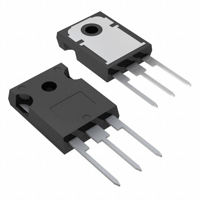
STW6N120K3
Single FETs, MOSFETs


.png?x-oss-process=image/format,webp/resize,p_30)


STW6N120K3 Description
STW6N120K3 Description
The STW6N120K3 is a high-performance MOSFET (Metal Oxide) from STMicroelectronics, designed for demanding applications that require high voltage and current handling capabilities. With a drain to source voltage (Vdss) of 1200V and a continuous drain current (Id) of 6A at 25°C, this N-CH device is well-suited for applications in power electronics, industrial control, and automotive systems.
STW6N120K3 Features
- High Voltage and Current Handling: The STW6N120K3 can handle a maximum drain to source voltage of 1200V and a continuous drain current of 6A at 25°C, making it ideal for high-power applications.
- Low On-Resistance: The device features a maximum on-resistance (Rds On) of 2.4Ω at 2.5A and 10V, ensuring efficient power dissipation and reduced power loss.
- Robust Gate Drive: With a maximum gate-source voltage (Vgs) of ±30V and a threshold voltage (Vgs(th)) of 5V at 100µA, the STW6N120K3 offers reliable gate control and operation.
- Low Input Capacitance: The device has a maximum input capacitance (Ciss) of 1050 pF at 100V, contributing to faster switching speeds and reduced parasitic effects.
- Low Gate Charge: The maximum gate charge (Qg) is 34 nC at 10V, enabling efficient gate drive and reduced power consumption.
- Compliance and Environmental: The STW6N120K3 is compliant with RoHS3 and REACH regulations, making it suitable for environmentally conscious applications.
STW6N120K3 Applications
- Power Electronics: The STW6N120K3's high voltage and current ratings make it ideal for power conversion, motor control, and power supply applications.
- Industrial Control: Its robust performance characteristics make it suitable for use in industrial automation, robotics, and process control systems.
- Automotive Systems: The device's ability to handle high voltages and currents, along with its low on-resistance, makes it well-suited for automotive applications such as electric vehicle charging systems and power management.
Conclusion of STW6N120K3
The STW6N120K3 is a versatile and high-performance MOSFET from STMicroelectronics, offering a combination of high voltage and current handling capabilities, low on-resistance, and robust gate drive. Its compliance with environmental regulations and suitability for a wide range of applications make it an excellent choice for power electronics, industrial control, and automotive systems. However, it is important to note that the STW6N120K3 is currently classified as obsolete, which may impact its availability and long-term support.
Tech Specifications
STW6N120K3 Documents
Download datasheets and manufacturer documentation for STW6N120K3
 IPG-PWR/14/8674 02/Sep/2014
  ST(FW,P,W)6N120K3
  IRF630 View All Specifications
  Mult Devices OBS 22/Jan/2018
  ST(FW,P,W)6N120K3
 Shopping Guide


.png?x-oss-process=image/format,webp/resize,h_32)


