
 German
 Japanese
 Portuguese
 Korea
Korea
 Mexico
 Dutch
Dutch


STMicroelectronics
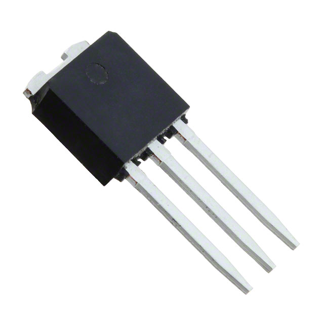
STU6NF10
Why Choose Us?
Professional Platform
B2B & B2C purchasingDelivery at full speed
1-2 days deliveryWide variety
Original manufacturers365 days guarantee
Responsible quality
.png)


Tech Specifications
STU6NF10 Description
STU6NF10 Description
The STU6NF10 is a high-performance N-Channel MOSFET from STMicroelectronics, designed for applications requiring high power and efficiency. With a drain-to-source voltage of 100V and a continuous drain current of 6A at 25°C, this device is capable of handling demanding power electronic applications. The STU6NF10 features a low on-resistance of 250mOhm at 3A and 10V, ensuring minimal power dissipation and high efficiency. The device is housed in an IPAK package, making it suitable for through-hole mounting in various electronic systems.
STU6NF10 Features
- Low On-Resistance: The STU6NF10 boasts a low on-resistance of 250mOhm at 3A and 10V, which minimizes power dissipation and improves efficiency in power electronic applications.
- High Drain-to-Source Voltage: With a drain-to-source voltage of 100V, this MOSFET can handle high voltage applications, making it suitable for various power electronic systems.
- High Continuous Drain Current: The STU6NF10 can handle a continuous drain current of 6A at 25°C, ensuring reliable performance in demanding applications.
- Low Gate Charge: The device has a low gate charge of 14nC at 10V, reducing switching losses and improving overall efficiency.
- Robust Input Capacitance: The STU6NF10 features an input capacitance of 280pF at 25V, ensuring stable operation and reducing noise in high-frequency applications.
- Compliance with Industry Standards: The device is compliant with RoHS3 and REACH standards, making it suitable for environmentally conscious applications.
STU6NF10 Applications
The STU6NF10 is ideal for a wide range of applications, including:
- Power Supplies: Due to its high voltage and current ratings, the STU6NF10 is well-suited for power supply applications, such as switching power supplies and battery chargers.
- Motor Control: The device's low on-resistance and high current capabilities make it an excellent choice for motor control applications, including electric vehicles and industrial motor drives.
- Industrial Automation: The STU6NF10's robust performance and compliance with industry standards make it suitable for use in industrial automation systems, such as robotics and control systems.
- Renewable Energy Systems: The device's high voltage and current ratings, combined with its low on-resistance, make it ideal for use in renewable energy systems, such as solar inverters and wind power converters.
Conclusion of STU6NF10
The STU6NF10 is a versatile and high-performance N-Channel MOSFET from STMicroelectronics, offering a combination of low on-resistance, high voltage and current ratings, and compliance with industry standards. Its unique features and advantages make it an ideal choice for a wide range of power electronic applications, including power supplies, motor control, industrial automation, and renewable energy systems. With its robust performance and compliance with environmental standards, the STU6NF10 is a reliable and efficient solution for demanding electronic systems.
FAQ
| Quantity | Unit Price | Ext. Price |
|---|---|---|
| 1+ | $1.35085 | $1.35 |
| 10+ | $1.32172 | $13.22 |
| 30+ | $1.30285 | $39.09 |
Not available to buy online? Want the lower wholesale price? Please Send RFQ to get best price, we will respond immediately


.png?x-oss-process=image/format,webp/resize,h_32)


