
 German
 Japanese
 Portuguese
 Korea
Korea
 Mexico
 Dutch
Dutch


Texas Instruments
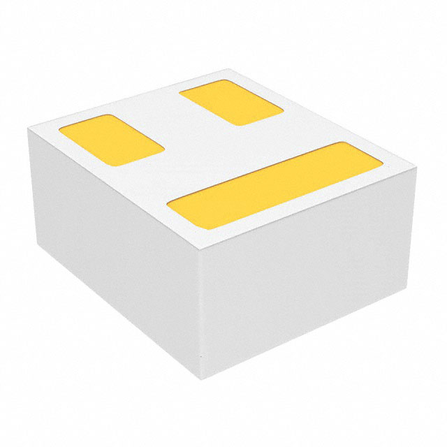
CSD15380F3T

Why Choose Us?
Professional Platform
B2B & B2C purchasingDelivery at full speed
1-2 days deliveryWide variety
Original manufacturers365 days guarantee
Responsible quality
.png)


Tech Specifications
CSD15380F3T Description
CSD15380F3T Description
The CSD15380F3T from Texas Instruments is a N-channel FemtoFET™ MOSFET designed for high-efficiency, low-power applications. With a drain-to-source voltage (Vdss) of 20V and a continuous drain current (Id) of 500mA, this surface-mount device is optimized for space-constrained designs. It features an ultra-low input capacitance (Ciss) of 10.5 pF @ 10V and a gate charge (Qg) of just 0.281 nC @ 10V, enabling fast switching and reduced power losses. The Rds(on) of 1190mΩ @ 100mA, 8V ensures efficient conduction, while its 1.35V threshold voltage (Vgs(th)) makes it compatible with low-voltage logic. Packaged in 3-pin PICOSTAR™ (Tape & Reel), it is ideal for portable and battery-powered systems.
CSD15380F3T Features
- Ultra-Compact Design: FemtoFET™ technology minimizes footprint, perfect for high-density PCBs.
- Low Gate Charge & Capacitance: Enhances switching efficiency, reducing energy losses in high-frequency applications.
- Low Threshold Voltage (1.35V): Compatible with 1.8V/3.3V logic levels, eliminating need for gate drivers.
- RoHS3 & REACH Compliant: Meets environmental and regulatory standards for global use.
- 500mW Power Dissipation: Reliable thermal performance in compact layouts.
- MSL1 (Unlimited): No baking required, simplifying assembly processes.
CSD15380F3T Applications
- Portable Electronics: Smartphones, wearables, and IoT devices benefit from its low power and small size.
- Power Management: Load switches, DC-DC converters, and battery protection circuits.
- Signal Switching: High-speed data multiplexing and analog switching.
- Embedded Systems: Low-voltage microcontrollers and sensor interfaces.
Conclusion of CSD15380F3T
The CSD15380F3T stands out for its miniaturized form factor, low-power operation, and high switching efficiency, making it a superior choice for modern electronics. Its FemtoFET™ architecture outperforms traditional MOSFETs in space-constrained designs, while its low gate drive requirements simplify circuit design. Whether for consumer gadgets or industrial systems, this MOSFET delivers reliability, efficiency, and compliance with stringent environmental standards.
FAQ
| Quantity | Unit Price | Ext. Price |
|---|---|---|
| 5+ | $0.14479 | $0.72 |
| 50+ | $0.11516 | $5.76 |
| 250+ | $0.10036 | $25.09 |
Not available to buy online? Want the lower wholesale price? Please Send RFQ to get best price, we will respond immediately


.png?x-oss-process=image/format,webp/resize,h_32)


