Texas Instruments_CSD18503Q5A

Texas Instruments
CSD18503Q5A  
Single FETs, MOSFETs

Texas Instruments
CSD18503Q5A
278-CSD18503Q5A
Ersa
Texas Instruments-CSD18503Q5A-datasheets-7314346.pdf
MOSFET N-CH 40V 19A/100A 8VSON
In Stock : 9878

Not available to buy online? Want the lower wholesale price? Please Send RFQ to get best price, we will respond immediately

QUICK RFQ
ADD TO RFQ LIST
ersa FreeSample ersa flow
  • Quantity
  • Unit Price
  • Ext. Price
    • 1+
    • $1.27678
    • $1.28
    • 10+
    • $1.06481
    • $10.65
    • 30+
    • $0.94889
    • $28.47
    ADD TO CART
    QUICK ORDER
    $1.27678    $1.28
    ISO9001
    Quality Policy
    ISO45001
    ISO14001

    CSD18503Q5A Description

    The Texas Instruments CSD18503Q5A is a highly-integrated, high-voltage gate driver with advanced features that enable efficient and reliable control of power switches in a wide range of applications.

    Description:

    The CSD18503Q5A is a monolithic, high-voltage half-bridge gate driver that provides isolated control of two external power switches. It is designed to operate from a supply voltage as low as 4.75V and can handle high-side and low-side N-type MOSFETs with voltage ratings up to 900V. The device features a robust, high-voltage, isolated gate drive with a peak current of ±2A and a propagation delay of only 18ns.

    Features:

    • Integrated high-voltage half-bridge gate driver
    • Supports N-type MOSFETs up to 900V
    • Operates from a supply voltage as low as 4.75V
    • ±2A peak current capability
    • Propagation delay of only 18ns
    • Robust, isolated gate drive
    • Integrated high-side and low-side gate drivers
    • Independent control of high-side and low-side switches
    • Short circuit protection and over-current protection
    • Thermal shutdown and over-temperature warning
    • Spread spectrum frequency modulation to reduce EMI
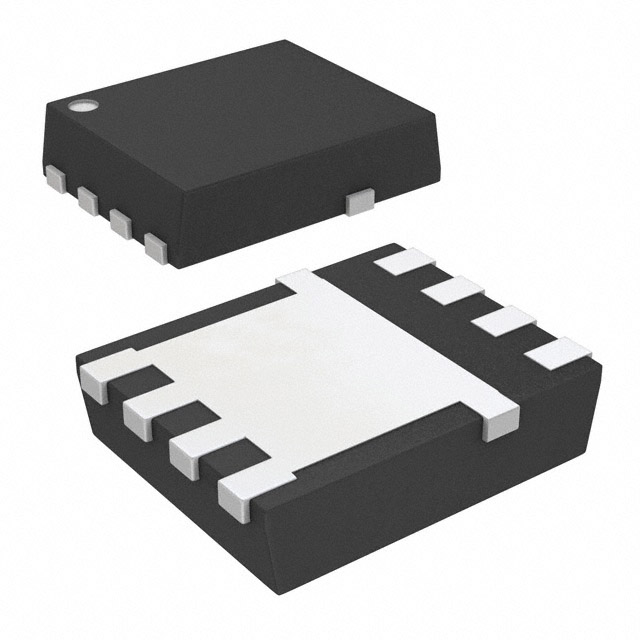
    • Small, 5mm x 7mm QFN package

    Applications:

    The CSD18503Q5A is suitable for a wide range of power conversion applications, including:

    1. Motor control: Brushless DC (BLDC) motors, permanent magnet synchronous motors (PMSM), and induction motors.
    2. Power supply: AC-DC and DC-DC converters, including isolated and non-isolated topologies.
    3. Renewable energy: Solar inverters, battery chargers, and energy storage systems.
    4. Industrial control: Servo drives, variable frequency drives (VFDs), and robotics.
    5. Automotive: Electric vehicle (EV) and hybrid electric vehicle (HEV) powertrains, including traction inverters and onboard chargers.

    In summary, the Texas Instruments CSD18503Q5A is a versatile and efficient high-voltage gate driver that can be used in a wide range of power conversion applications. Its advanced features, such as robust gate drive, propagation delay, and integrated protection, make it an ideal choice for demanding applications requiring high performance and reliability.

    Tech Specifications

    Configuration
    Typical Turn-Off Delay Time (ns)
    Maximum Gate Source Leakage Current (nA)
    Input Capacitance (Ciss) (Max) @ Vds
    Gate Charge (Qg) (Max) @ Vgs
    Typical Rise Time (ns)
    PPAP
    Channel Mode
    Typical Turn-On Delay Time (ns)
    Product Status
    Automotive
    Drain to Source Voltage (Vdss)
    Supplier Package
    Maximum IDSS (uA)
    Package / Case
    Technology
    REACH Status
    Channel Type
    EU RoHS
    Maximum Continuous Drain Current (A)
    Moisture Sensitivity Level (MSL)
    Operating Temperature
    Maximum Pulsed Drain Current @ TC=25°C (A)
    Maximum Drain Source Voltage (V)
    Maximum Drain Source Resistance (mOhm)
    ECCN
    Mounting Type
    Rds On (Max) @ Id, Vgs
    Standard Package Name
    Vgs(th) (Max) @ Id
    Typical Reverse Recovery Charge (nC)
    Maximum Continuous Drain Current on PCB @ TC=25°C (A)
    Pin Count
    Mounting
    Minimum Gate Threshold Voltage (V)
    Typical Reverse Transfer Capacitance @ Vds (pF)
    Lead Shape
    Current - Continuous Drain (Id) @ 25°C
    Typical Gate to Drain Charge (nC)
    SVHC
    Drive Voltage (Max Rds On, Min Rds On)
    HTSUS
    Package
    Typical Gate Charge @ Vgs (nC)
    Typical Input Capacitance @ Vds (pF)
    Maximum Power Dissipation on PCB @ TC=25°C (W)
    Category
    Maximum Gate Resistance (Ohm)
    PCB changed
    HTS
    FET Type
    Number of Elements per Chip
    Typical Reverse Recovery Time (ns)
    ECCN (US)
    Maximum Power Dissipation (mW)
    Supplier Device Package
    Minimum Operating Temperature (°C)
    Maximum Operating Temperature (°C)
    Power Dissipation (Max)
    Typical Fall Time (ns)
    Process Technology
    Package Height
    Typical Gate to Source Charge (nC)
    Maximum Positive Gate Source Voltage (V)
    Mfr
    Vgs (Max)
    Typical Drain Source Resistance @ 25°C (mOhm)
    RoHS Status
    Typical Gate Threshold Voltage (V)
    FET Feature
    Maximum Gate Source Voltage (V)
    SVHC Exceeds Threshold
    Typical Gate Plateau Voltage (V)
    Material
    Package Length
    Typical Gate Charge @ 10V (nC)
    Maximum Diode Forward Voltage (V)
    Series
    Typical Diode Forward Voltage (V)
    Operating Junction Temperature (°C)
    Typical Output Capacitance (pF)
    Part Status
    Maximum Gate Threshold Voltage (V)
    Package Width
    Maximum Junction Ambient Thermal Resistance on PCB (°C/W)
    Base Product Number
    Unit Weight
    Id - Continuous Drain Current
    Fall Time
    RoHS
    Qg - Gate Charge
    Tradename
    Transistor Type
    Number of Channels
    Typical Turn-On Delay Time
    Height
    Maximum Operating Temperature
    Width
    Rds On - Drain-Source Resistance
    Mounting Style
    Vgs - Gate-Source Voltage
    Typical Turn-Off Delay Time
    Transistor Polarity
    Minimum Operating Temperature
    Vds - Drain-Source Breakdown Voltage
    Rise Time
    Length
    Forward Transconductance - Min
    Vgs th - Gate-Source Threshold Voltage
    Pd - Power Dissipation
    USHTS

    CSD18503Q5A Documents

    Download datasheets and manufacturer documentation for CSD18503Q5A

    Ersa CSD18503Q5A Datasheet      
    Ersa CSD18503Q5A Datasheet      

    Shopping Guide

    Payment Methods
    Payment Methods include Prepayment TT (bank transfer), Western Union, and PayPal. Customers are responsible for shipping costs, bank charges, customs duties and taxes.
    Shipping Rate
    Shipments are made once a day around 5pm, excluding Sundays. Once shipped, the estimated delivery time is usually 5-7 business days, depending on the courier you choose.
    Delivery Methods
    Provide DHL, FedEx, UPS, EMS, SF Express and Registered Airmail International Delivery Service