

Texas Instruments
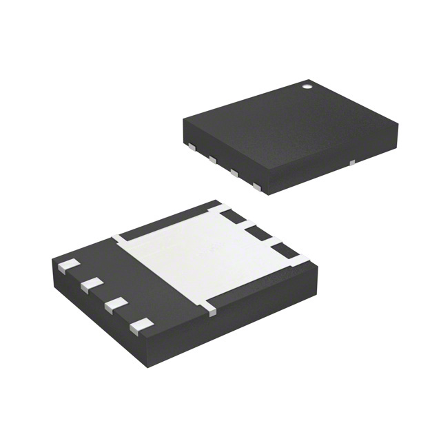
CSD18532NQ5B
Single FETs, MOSFETs

Not available to buy online? Want the lower wholesale price? Please Send RFQ to get best price, we will respond immediately


- 1+
- $2.60489
- $2.6
- 10+
- $2.04185
- $20.42
- 30+
- $1.70734
- $51.22

.png?x-oss-process=image/format,webp/resize,p_30)


CSD18532NQ5B Description
CSD18532NQ5B Description
The CSD18532NQ5B is a high-performance N-Channel MOSFET from Texas Instruments, designed for applications requiring high efficiency and reliability. This device features a NexFET™ series, which is known for its excellent electrical characteristics and robustness. With a drain-to-source voltage (Vdss) of 60V and a continuous drain current (Id) of 22A at 25°C and 100A at Tc, the CSD18532NQ5B is suitable for a wide range of power management and motor control applications.
CSD18532NQ5B Features
- NexFET™ Series: Offers superior electrical performance and robustness.
- 60V Drain-to-Source Voltage (Vdss): Suitable for high-voltage applications.
- 22A Continuous Drain Current (Id) at 25°C and 100A at Tc: Capable of handling high current loads.
- 3.4mOhm Rds On (Max) @ 25A, 10V: Low on-resistance for high efficiency.
- 3.4V Vgs(th) (Max) @ 250µA: Ensures reliable turn-on and turn-off.
- 64 nC Gate Charge (Qg) (Max) @ 10V: Minimizes power loss and improves efficiency.
- ±20V Vgs (Max): Provides a wide voltage range for gate control.
- 5340 pF Input Capacitance (Ciss) (Max) @ 30V: Minimizes capacitive effects.
- 3.2W Power Dissipation (Max) (Ta): Capable of dissipating heat effectively.
- Surface Mount Mounting Type: Ideal for space-constrained applications.
- ROHS3 Compliant: Meets environmental regulations.
- REACH Unaffected: Compliant with European chemical regulations.
- Moisture Sensitivity Level (MSL) 1 (Unlimited): Suitable for various environmental conditions.
CSD18532NQ5B Applications
The CSD18532NQ5B is ideal for a variety of applications where high efficiency, reliability, and performance are critical. Some specific use cases include:
- Power management systems: Due to its low on-resistance and high current capability, the CSD18532NQ5B is well-suited for power management applications, such as battery management and power conversion systems.
- Motor control: The high voltage and current ratings make it an excellent choice for motor control applications, including brushless DC motors and stepper motors.
- Industrial automation: The robustness and reliability of the NexFET™ series make the CSD18532NQ5B ideal for industrial automation applications, such as robotic actuators and control systems.
- Renewable energy systems: The device's high voltage and current ratings make it suitable for renewable energy systems, such as solar inverters and wind power converters.
Conclusion of CSD18532NQ5B
The CSD18532NQ5B is a high-performance N-Channel MOSFET from Texas Instruments, offering excellent electrical characteristics, robustness, and reliability. Its NexFET™ series design, combined with its high voltage and current ratings, make it an ideal choice for a wide range of power management, motor control, and industrial automation applications. With its low on-resistance and compliance with environmental regulations, the CSD18532NQ5B is a reliable and efficient solution for demanding applications.
Tech Specifications
CSD18532NQ5B Documents
Download datasheets and manufacturer documentation for CSD18532NQ5B
Function Diagram Product change notification (PDF) PROCESS CHANGE NOTIFICATION (PDF) Qualification of Reduced Wire Bond diameter for the Family of Discrete Clip & Power Block Devices (PDF) Qualification of TI Clark as additional Assembly site for selected VSON packaged products (PDF) Product Change Notification (PDF) CSD18532NQ5B PSpice Model (Rev. B) Related Parts


Shopping Guide


.png?x-oss-process=image/format,webp/resize,h_32)


©2025 ERSA Electronics Corporation.