

Texas Instruments
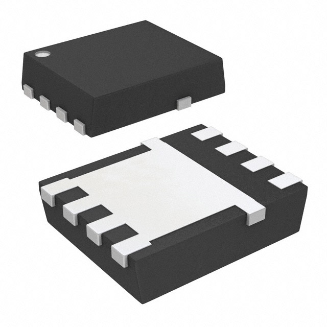
CSD17555Q5A
Single FETs, MOSFETs

Not available to buy online? Want the lower wholesale price? Please Send RFQ to get best price, we will respond immediately


.png?x-oss-process=image/format,webp/resize,p_30)


CSD17555Q5A Description
CSD17555Q5A Description
The CSD17555Q5A is a high-performance N-Channel MOSFET from Texas Instruments, designed for applications requiring high efficiency and low power dissipation. With a drain-to-source voltage of 30V and continuous drain current ratings of 24A at 25°C and 100A at case temperature, this device is well-suited for a variety of power management and motor control applications.
CSD17555Q5A Features
- High Input Capacitance (Ciss): The CSD17555Q5A boasts an impressive input capacitance of 4650 pF at 15V, which helps reduce switching losses and improve overall system efficiency.
- Low Gate Charge (Qg): With a maximum gate charge of 28 nC at 4.5V, this MOSFET minimizes power dissipation during switching, contributing to longer device life and reduced thermal management requirements.
- Robust Voltage Ratings: The device can handle gate-source voltages up to ±20V, providing flexibility in various circuit designs.
- Low On-Resistance (Rds On): At 25A and 10V, the CSD17555Q5A exhibits a low on-resistance of 2.7mOhm, which minimizes power losses and improves efficiency in high-current applications.
- Surface Mount Technology: The surface mount packaging allows for compact and efficient PCB layouts, ideal for space-constrained designs.
- Compliance and Certifications: The CSD17555Q5A is REACH Unaffected and RoHS3 Compliant, ensuring environmental and regulatory compliance in various markets.
CSD17555Q5A Applications
The CSD17555Q5A is an ideal choice for applications where high efficiency and robust performance are critical:
- Power Management: In power supply designs, the low on-resistance and high current ratings make it suitable for high-efficiency power conversion.
- Motor Control: The device's ability to handle high currents and voltages makes it an excellent choice for motor drivers in industrial and automotive applications.
- Automotive: Due to its high current and voltage capabilities, the CSD17555Q5A is well-suited for automotive applications such as electric power steering and battery management systems.
Conclusion of CSD17555Q5A
The CSD17555Q5A from Texas Instruments stands out for its combination of high input capacitance, low gate charge, and robust voltage ratings, making it a top choice for demanding power management and motor control applications. Its unique features, such as low on-resistance and compliance with environmental standards, further enhance its appeal in the electronics industry. With its NexFET™ series pedigree, the CSD17555Q5A delivers superior performance and reliability, making it a preferred choice for engineers designing cutting-edge electronic systems.
Tech Specifications
CSD17555Q5A Documents
Download datasheets and manufacturer documentation for CSD17555Q5A
CSD17555Q5A CSD17555Q5A Related Parts


Shopping Guide


.png?x-oss-process=image/format,webp/resize,h_32)


©2025 ERSA Electronics Corporation.