
 German
 Japanese
 Portuguese
 Korea
Korea
 Mexico
 Dutch
Dutch


Texas Instruments
CSD18510KTT
278-CSD18510KTT

PDF Datasheet
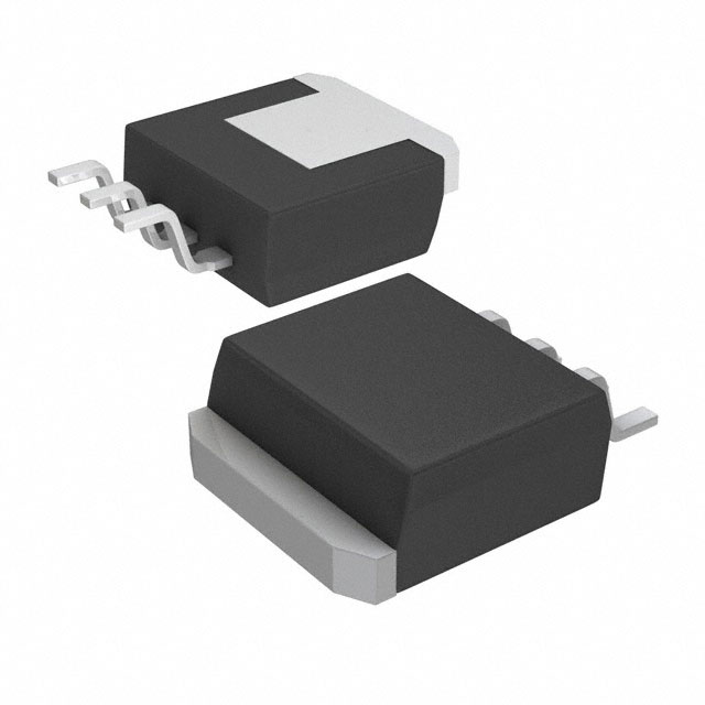
40V, N ch NexFET MOSFET™, single D2PAK, 1.7mOhm 3-DDPAK/TO-263 -55 to 175
6 Weeks
Why Choose Us?
Professional Platform
B2B & B2C purchasingDelivery at full speed
1-2 days deliveryWide variety
Original manufacturers365 days guarantee
Responsible quality
.png)


Tech Specifications
Number of Terminals
2
Terminal Position
SINGLE
JEDEC Package Code
TO-263AB
Number of Elements
1
RoHS
No
Eccn Code
EAR99
Lead Free
Yes
REACH
not_compliant
CSD18510KTT Description
N-Channel 40 V 274A (Tc) 250W (Ta) Surface Mount TO-263 (DDPAK-3)
FAQ
Does CSD18510KTT have quantity-based pricing?
Yes. CSD18510KTT currently has 3 pricing tier(s), starting from 1 units.
What is the standard lead time for CSD18510KTT?
What is CSD18510KTT?
Is CSD18510KTT currently in stock?
What package or case is CSD18510KTT available in?
Availability
(In Stock :
11 )
| Quantity | Unit Price | Ext. Price |
|---|---|---|
| 1+ | $2.33143 | $2.33 |
| 10+ | $2.07772 | $20.78 |
| 30+ | $1.89772 | $56.93 |
ADD TO CART
QUICK ORDER
Unit Price $2.33143
Subtotal $2.33
Quick Quote
ADD TO RFQ LIST
Not available to buy online? Want the lower wholesale price? Please Send RFQ to get best price, we will respond immediately
QUICK RFQ


.png?x-oss-process=image/format,webp/resize,h_32)


