

Texas Instruments
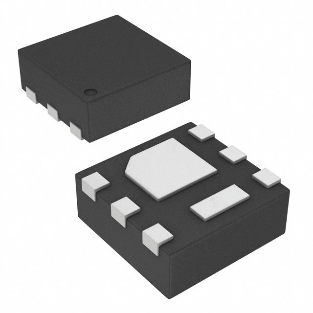
CSD17313Q2T
Single FETs, MOSFETs

Not available to buy online? Want the lower wholesale price? Please Send RFQ to get best price, we will respond immediately


.png?x-oss-process=image/format,webp/resize,p_30)


CSD17313Q2T Description
The CSD17313Q2T is a high-performance, low-voltage, gate driver with integrated power MOSFETs from Texas Instruments. It is designed to drive external MOSFETs in a variety of applications, including motor control, automotive systems, and industrial control.
Description:
The CSD17313Q2T is a monolithic gate driver IC that integrates two low-side N-channel power MOSFETs and a high-speed gate driver. It is available in a compact 16-pin QFN package, making it suitable for space-constrained applications.
Features:
- Integrated high-speed gate driver: The CSD17313Q2T features a high-speed gate driver that can drive external MOSFETs with fast switching times and low propagation delays.
- Low-side N-channel power MOSFETs: The device includes two low-side N-channel power MOSFETs with low on-resistance and low gate charge, providing efficient switching performance.
- Wide input voltage range: The CSD17313Q2T can operate over a wide input voltage range of 4.75V to 18V, making it suitable for various applications with different supply voltages.
- Advanced protection features: The device offers several protection features, including overcurrent protection, overtemperature protection, and short-circuit protection, ensuring reliable operation and system safety.
- Spread spectrum frequency modulation: The CSD17313Q2T features spread spectrum frequency modulation to reduce electromagnetic interference (EMI) and improve system performance.
- Small package size: The 16-pin QFN package allows for easy integration into compact designs.
Applications:
- Motor control: The CSD17313Q2T is ideal for driving external MOSFETs in brushless DC (BLDC) motor control applications, providing efficient switching and control.
- Automotive systems: The device can be used in automotive systems, such as electric power steering (EPS) and window lift applications, where high performance and reliability are required.
- Industrial control: The CSD17313Q2T is suitable for various industrial control applications, including robotics, conveyor systems, and factory automation equipment.
- Battery management systems: The device can be used in battery management systems to drive MOSFETs for efficient battery charging and protection.
- Power supplies: The CSD17313Q2T can be used in power supply applications, such as switched-mode power supplies (SMPS) and battery chargers, to drive external MOSFETs for efficient power conversion.
In summary, the CSD17313Q2T from Texas Instruments is a versatile, high-performance gate driver IC with integrated power MOSFETs, designed for a wide range of applications, including motor control, automotive systems, and industrial control. Its compact package size, advanced protection features, and wide input voltage range make it an ideal choice for space-constrained and high-reliability applications.
Tech Specifications
CSD17313Q2T Documents
Download datasheets and manufacturer documentation for CSD17313Q2T
CSDYYY 01/Feb/2019 CSD17313Q2 TI Solutions Tablets,eBooks Power Management Guide CSD17313Q2 Related Parts


Shopping Guide


.png?x-oss-process=image/format,webp/resize,h_32)


©2025 ERSA Electronics Corporation.