

Texas Instruments
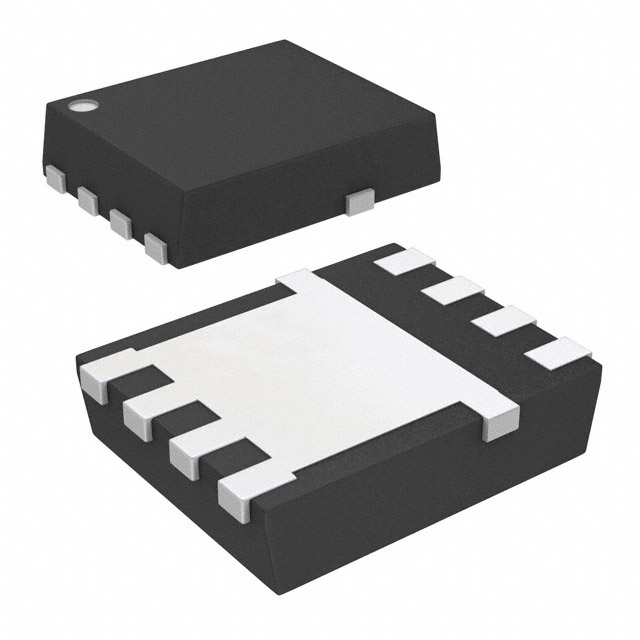
CSD16325Q5
Single FETs, MOSFETs

Not available to buy online? Want the lower wholesale price? Please Send RFQ to get best price, we will respond immediately


.png?x-oss-process=image/format,webp/resize,p_30)


CSD16325Q5 Description
CSD16325Q5 Description
The CSD16325Q5 is a high-performance N-Channel MOSFET designed and manufactured by Texas Instruments. It features a NexFET™ series, offering superior performance in various applications. With a maximum drain-to-source voltage (Vdss) of 25V and a continuous drain current (Id) of 33A at 25°C and 100A at case temperature, this MOSFET is ideal for high-power applications. The device is surface-mountable and comes in a tape and reel (TR) packaging, making it suitable for automated assembly processes.
CSD16325Q5 Features
- NexFET™ Series: Offers improved performance and reliability compared to traditional MOSFETs.
- Maximum Drain-to-Source Voltage (Vdss): 25V
- Continuous Drain Current (Id): 33A at 25°C and 100A at case temperature
- Maximum Power Dissipation (Pd): 3.1W (Ta)
- Low Rds On (Max): 2mOhm at 30A, 8V
- Maximum Gate Charge (Qg): 25nC at 4.5V
- Maximum Input Capacitance (Ciss): 4000pF at 12.5V
- Maximum Drive Voltage: 3V (Max Rds On) and 8V (Min Rds On)
- Vgs(th) (Max): 1.4V at 250µA
- Moisture Sensitivity Level (MSL): 1 (Unlimited)
- REACH Unaffected and ROHS3 Compliant
- ECCN: EAR99
- HTSUS: 8541.29.0095
CSD16325Q5 Applications
The CSD16325Q5 is ideal for various high-power applications, including:
- Motor control and drives
- Power management systems
- Renewable energy applications, such as solar inverters
- Industrial automation and control systems
- Automotive electronics, such as electric vehicle chargers and powertrain control
- High-efficiency power supplies and converters
Conclusion of CSD16325Q5
The CSD16325Q5 is a high-performance N-Channel MOSFET from Texas Instruments, offering superior performance and reliability in high-power applications. Its NexFET™ series, low Rds On, and high drain current capabilities make it an excellent choice for motor control, power management, and renewable energy applications. With its REACH unaffected and ROHS3 compliant status, the CSD16325Q5 is an environmentally friendly solution for your high-power electronic designs.
Tech Specifications
CSD16325Q5 Documents
Download datasheets and manufacturer documentation for CSD16325Q5
Assembly/Test Site Revision C 09/Feb/2015 CSD16325Q5 CSD16325Q5 Qualification Revision A 01/Jul/2014 Related Parts


Shopping Guide


.png?x-oss-process=image/format,webp/resize,h_32)


©2025 ERSA Electronics Corporation.