
Texas Instruments
CSD25213W10
Single FETs, MOSFETs


.png?x-oss-process=image/format,webp/resize,p_30)


CSD25213W10 Description
CSD25213W10 is a high-performance, single-channel, synchronous, step-down (buck) regulator from Texas Instruments. It is designed to provide efficient power conversion for a wide range of applications, including automotive, industrial, and consumer electronics.
Description:
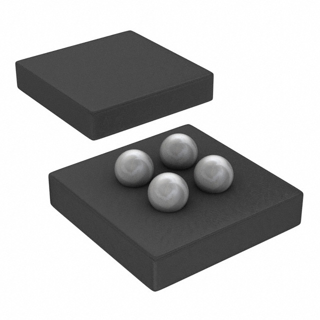
The CSD25213W10 is a highly integrated, high-density power module that offers high efficiency and low thermal resistance. It features a compact, thermally efficient package that allows for easy integration into a variety of applications.
Features:
- High Efficiency: The CSD25213W10 offers high efficiency of up to 96%, which helps to reduce power consumption and improve overall system performance.
- Wide Input Voltage Range: The device can operate with an input voltage range of 4.5V to 28V, making it suitable for a wide range of applications.
- High Output Current: The CSD25213W10 can deliver up to 10A of continuous output current, making it suitable for high-current applications.
- Synchronous Rectification: The device uses synchronous rectification to improve efficiency and reduce power loss.
- High-Density Integration: The CSD25213W10 is available in a compact, thermally efficient package that allows for easy integration into a variety of applications.
- Protection Features: The device offers over-current protection, over-temperature protection, and under-voltage lockout to ensure safe and reliable operation.
Applications:
The CSD25213W10 is suitable for a wide range of applications, including:
- Automotive: Infotainment systems, power windows, and LED lighting.
- Industrial: Motor drives, industrial control systems, and medical equipment.
- Consumer Electronics: Portable devices, smartphones, and laptops.
- Telecommunications: Base stations, routers, and network switches.
In summary, the CSD25213W10 is a high-performance, single-channel, synchronous, step-down regulator that offers high efficiency, a wide input voltage range, and high output current. It is suitable for a variety of applications, including automotive, industrial, and consumer electronics.
Tech Specifications
CSD25213W10 Documents
Download datasheets and manufacturer documentation for CSD25213W10
 CSD25213W10
  Carrier Tape 28/Aug/2018
  CSD25213W10
  DSBGA/Usip 14/Sep/2016 DSBGA/uSIP 22/Jun/2016
 Shopping Guide


.png?x-oss-process=image/format,webp/resize,h_32)


