
 German
 Japanese
 Portuguese
 Korea
Korea
 Mexico
 Dutch
Dutch


Texas Instruments
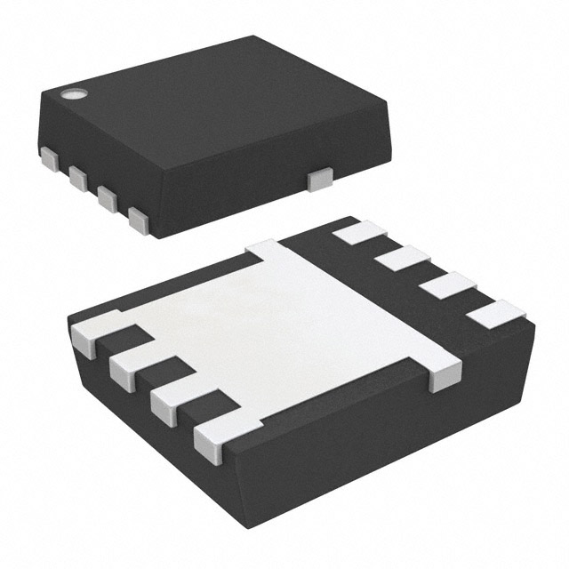
CSD18514Q5A

Why Choose Us?
Professional Platform
B2B & B2C purchasingDelivery at full speed
1-2 days deliveryWide variety
Original manufacturers365 days guarantee
Responsible quality
.png)


Tech Specifications
CSD18514Q5A Description
The Texas Instruments CSD18514Q5A is a highly integrated gate driver IC that is specifically designed for use in battery management systems (BMS) for electric vehicles (EVs) and hybrid electric vehicles (HEVs). It is a member of the company's portfolio of silicon carbide (SiC) power management solutions.
Description:
The CSD18514Q5A is a highly integrated gate driver IC that is designed to drive SiC MOSFETs in high-voltage applications. It features a compact, 5mm x 5mm QFN package and is designed to operate over a wide input voltage range of 4.75V to 60V. The device is capable of driving up to four SiC MOSFETs with a maximum current of ±10A per channel.
Features:
- Integrated gate driver for SiC MOSFETs
- Wide input voltage range of 4.75V to 60V
- Capable of driving up to four SiC MOSFETs
- Maximum current of ±10A per channel
- Compact 5mm x 5mm QFN package
- Designed for use in battery management systems for electric and hybrid vehicles
Applications:
The CSD18514Q5A is designed for use in high-voltage battery management systems for electric and hybrid vehicles. It is particularly well-suited for use in applications that require high efficiency and high reliability, such as in the powertrain systems of these vehicles. The device can also be used in other high-voltage applications that require efficient and reliable power management, such as in industrial motor drives and renewable energy systems.
Overall, the Texas Instruments CSD18514Q5A is a highly integrated gate driver IC that is specifically designed for use in high-voltage battery management systems for electric and hybrid vehicles. Its compact size, wide input voltage range, and ability to drive multiple SiC MOSFETs make it a versatile and efficient solution for these applications.
FAQ
Not available to buy online? Want the lower wholesale price? Please Send RFQ to get best price, we will respond immediately


.png?x-oss-process=image/format,webp/resize,h_32)


