
 German
 Japanese
 Portuguese
 Korea
Korea
 Mexico
 Dutch
Dutch


Texas Instruments
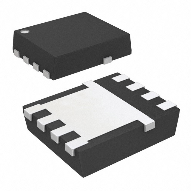
CSD16415Q5T

Why Choose Us?
Professional Platform
B2B & B2C purchasingDelivery at full speed
1-2 days deliveryWide variety
Original manufacturers365 days guarantee
Responsible quality
.png)


Tech Specifications
CSD16415Q5T Description
CSD16415Q5T Description
The CSD16415Q5T is a high-performance N-Channel MOSFET from Texas Instruments, designed for applications requiring high efficiency and fast switching speeds. This device features a NexFET™ series, which is known for its excellent electrical characteristics and robust performance. With a drain-source voltage (Vdss) of 25V and a continuous drain current (Id) of 100A at 25°C, the CSD16415Q5T is suitable for a wide range of power management and motor control applications.
CSD16415Q5T Features
- NexFET™ Series: Offers superior electrical performance and reliability compared to traditional MOSFETs.
- Low Rds On (1.15mOhm): Enables high efficiency and low power loss in high-current applications.
- High Input Capacitance (Ciss) of 4100 pF: Minimizes input charge and switching losses.
- Low Gate Charge (Qg) of 29 nC: Reduces switching losses and improves efficiency.
- Robust Drain to Source Voltage (Vdss) of 25V: Suitable for high-voltage applications.
- Continuous Drain Current (Id) of 100A at 25°C: Capable of handling high power loads.
- Drive Voltage (Max Rds On, Min Rds On) of 4.5V and 10V: Provides flexibility in gate drive requirements.
- Surface Mount Packaging: Ideal for space-constrained applications and high-density PCB layouts.
- REACH Unaffected and RoHS3 Compliant: Ensures environmental compliance and long-term availability.
CSD16415Q5T Applications
The CSD16415Q5T is ideal for a variety of applications where high efficiency, fast switching speeds, and robust performance are required. Some specific use cases include:
- Power management systems: The low Rds On and high Vdss make it suitable for power conversion and regulation in various electronic devices.
- Motor control applications: The high Id and low Qg enable efficient and fast control of electric motors in industrial and automotive applications.
- Renewable energy systems: The device's high efficiency and robust performance make it suitable for solar inverters and wind turbine control systems.
- Electric vehicles (EVs): The CSD16415Q5T can be used in EV charging systems, battery management, and motor control applications.
Conclusion of CSD16415Q5T
The CSD16415Q5T from Texas Instruments is a high-performance N-Channel MOSFET that offers excellent electrical characteristics, robust performance, and environmental compliance. Its unique features, such as low Rds On, high Ciss, and low Qg, make it an ideal choice for power management, motor control, and renewable energy applications. With its NexFET™ series advantages and wide range of applications, the CSD16415Q5T is a reliable and efficient solution for demanding electronic systems.
FAQ
| Quantity | Unit Price | Ext. Price |
|---|---|---|
| 1+ | $4.10572 | $4.11 |
| 10+ | $4.02000 | $40.20 |
| 30+ | $3.68400 | $110.52 |
Not available to buy online? Want the lower wholesale price? Please Send RFQ to get best price, we will respond immediately


.png?x-oss-process=image/format,webp/resize,h_32)


