
 German
 Japanese
 Portuguese
 Korea
Korea
 Mexico
 Dutch
Dutch


Texas Instruments
CSD23203W

Why Choose Us?
Professional Platform
B2B & B2C purchasingDelivery at full speed
1-2 days deliveryWide variety
Original manufacturers365 days guarantee
Responsible quality
.png)


Tech Specifications
CSD23203W Description
CSD23203W Description
The CSD23203W is a P-Channel MOSFET from Texas Instruments, designed for high-performance applications. This NexFET™ series device offers a unique combination of low on-resistance, high input capacitance, and low gate charge, making it ideal for a wide range of applications. With a drain-to-source voltage (Vdss) of 8V and a continuous drain current (Id) of 3A at 25°C, the CSD23203W delivers exceptional performance in demanding environments.
CSD23203W Features
- Low On-Resistance: The CSD23203W boasts a maximum Rds(on) of 19.4mΩ at 1.5A and 4.5V, ensuring minimal power loss and high efficiency.
- High Input Capacitance: With a maximum input capacitance (Ciss) of 914pF at 4V, this MOSFET provides fast switching speeds and improved transient response.
- Low Gate Charge: The maximum gate charge (Qg) of 6.3nC at 4.5V reduces switching losses and improves overall efficiency.
- Robust Power Dissipation: Capable of handling up to 750mW of power dissipation, the CSD23203W is suitable for high-power applications.
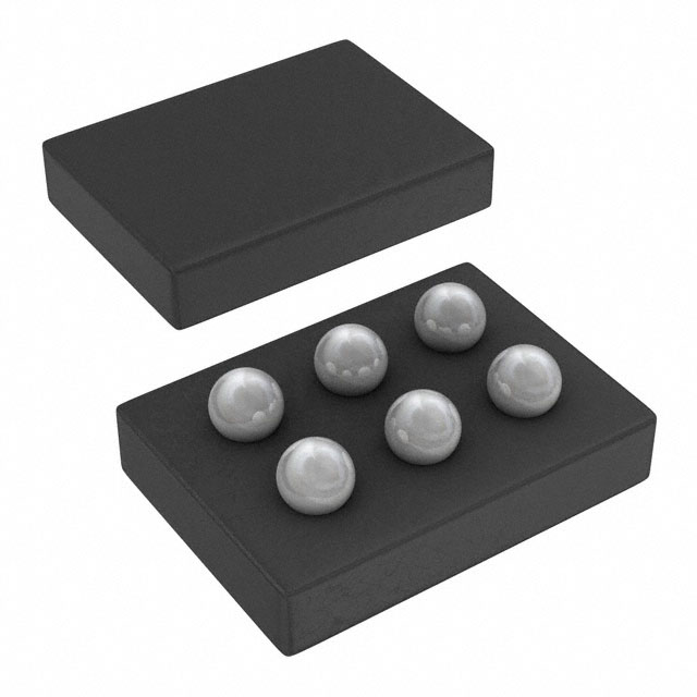
- Surface Mount Technology: The 6DSBGA package allows for easy integration into surface-mount applications, reducing footprint and improving thermal performance.
- Compliance and Certifications: The CSD23203W is REACH unaffected, RoHS3 compliant, and EAR99 classified, ensuring compliance with international regulations.
CSD23203W Applications
The CSD23203W is ideal for various applications where high performance and reliability are critical:
- Power Management: Due to its low on-resistance and high current handling capabilities, the CSD23203W is perfect for power management circuits in consumer electronics.
- Motor Control: Its ability to handle high voltages and currents makes it suitable for motor control applications in industrial and automotive systems.
- Automotive Applications: The robust power dissipation and high voltage ratings make the CSD23203W ideal for automotive electronics, such as power windows and seat controls.
- Industrial Control: The CSD23203W's high input capacitance and low gate charge make it suitable for high-speed switching in industrial control systems.
Conclusion of CSD23203W
The CSD23203W from Texas Instruments is a high-performance P-Channel MOSFET that offers a unique combination of low on-resistance, high input capacitance, and low gate charge. Its robust power dissipation, compliance with international regulations, and versatile applications make it an ideal choice for demanding applications in power management, motor control, automotive, and industrial control systems. With its NexFET™ technology, the CSD23203W delivers exceptional performance and reliability in a compact 6DSBGA package.
FAQ
Not available to buy online? Want the lower wholesale price? Please Send RFQ to get best price, we will respond immediately


.png?x-oss-process=image/format,webp/resize,h_32)


