

Texas Instruments
CSD19503KCS
Single FETs, MOSFETs

Not available to buy online? Want the lower wholesale price? Please Send RFQ to get best price, we will respond immediately


.png?x-oss-process=image/format,webp/resize,p_30)


CSD19503KCS Description
CSD19503KCS Description
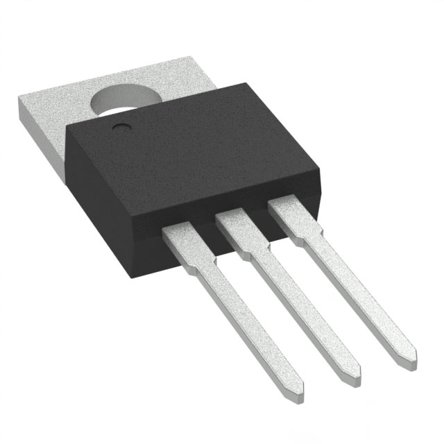
The CSD19503KCS from Texas Instruments is a high-performance N-channel MOSFET designed for power management applications requiring robust efficiency and thermal performance. Part of the NexFET™ series, it features an 80V drain-to-source voltage (Vdss) and a continuous drain current (Id) of 100A at 25°C, making it suitable for high-current switching. With an ultra-low on-resistance (Rds(on)) of 9.2mΩ at 60A and 10V gate drive, this MOSFET minimizes conduction losses, enhancing system efficiency. Packaged in a TO-220-3 through-hole format, it ensures reliable thermal dissipation, supporting a maximum power dissipation of 188W (Tc).
CSD19503KCS Features
- Low Rds(on): 9.2mΩ @ 60A, 10V reduces power losses in high-current applications.
- High Current Handling: 100A continuous drain current (Ta) for demanding power stages.
- Fast Switching: Optimized gate charge (Qg = 36nC @ 10V) and input capacitance (Ciss = 2730pF @ 40V) ensure efficient high-frequency operation.
- Wide Vgs Range: ±20V gate-to-source voltage tolerance enhances flexibility in drive circuitry.
- Robust Thermal Performance: TO-220-3 package with high power dissipation capability.
- Reliability: ROHS3 compliant, REACH unaffected, and MSL Not Applicable for industrial durability.
CSD19503KCS Applications
- DC-DC Converters: Ideal for synchronous buck/boost topologies due to low Rds(on) and high efficiency.
- Motor Drives: Suitable for H-bridge configurations in industrial and automotive systems.
- Power Supplies: High-current switching in server, telecom, and computing PSUs.
- Battery Management: Efficient power distribution in energy storage and EV charging systems.
- Industrial Automation: Robust performance in high-power switching applications like PLCs and inverters.
Conclusion of CSD19503KCS
The CSD19503KCS stands out as a high-efficiency, high-current MOSFET, combining low conduction losses, fast switching, and superior thermal management. Its 80V rating and 100A current capability make it a versatile choice for power electronics, while the NexFET™ technology ensures reliability in demanding environments. Whether used in DC-DC conversion, motor control, or industrial power systems, this MOSFET delivers optimal performance, making it a preferred solution for engineers prioritizing efficiency and durability.
Tech Specifications
CSD19503KCS Documents
Download datasheets and manufacturer documentation for CSD19503KCS
Site Chg 04/Dec/2015 CSD19503KCS CSD19503KCS Related Parts


Shopping Guide


.png?x-oss-process=image/format,webp/resize,h_32)


©2025 ERSA Electronics Corporation.