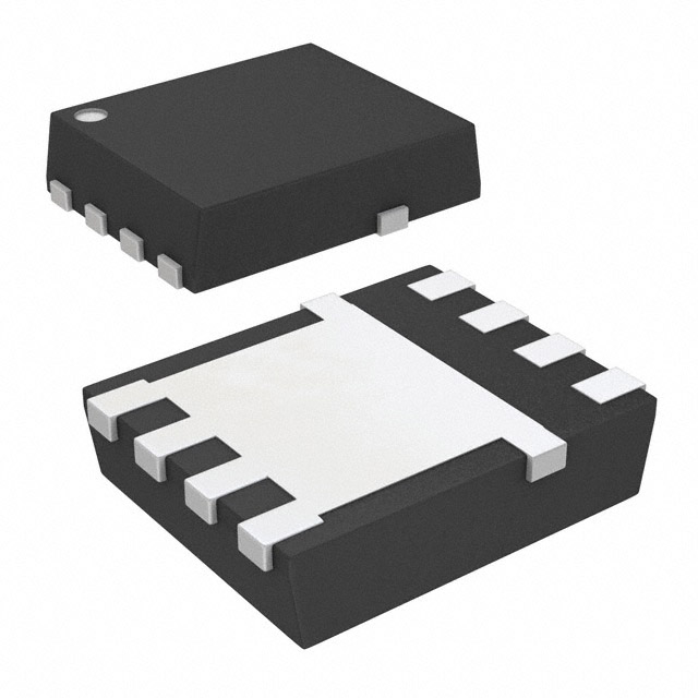
Texas Instruments_CSD19502Q5BT

Texas Instruments
CSD19502Q5BT  
Single FETs, MOSFETs

Texas Instruments
CSD19502Q5BT
278-CSD19502Q5BT
Ersa
Texas Instruments-CSD19502Q5BT-datasheets-3146411.pdf
MOSFET N-CH 80V 100A 8VSON
In Stock : 4206

Not available to buy online? Want the lower wholesale price? Please Send RFQ to get best price, we will respond immediately

QUICK RFQ
ADD TO RFQ LIST
ersa FreeSample ersa flow
ISO9001
Quality Policy
ISO45001
ISO14001

CSD19502Q5BT Description

The Texas Instruments CSD19502Q5BT is a highly-integrated, high-voltage half-bridge gate driver with integrated power MOSFETs. It is designed to drive external MOSFETs or IGBTs in a wide range of applications, including motor control, power conversion, and renewable energy systems.

Description:

The CSD19502Q5BT is a monolithic half-bridge gate driver with integrated power MOSFETs. It is designed to drive external MOSFETs or IGBTs in high-voltage applications. The device features a high-voltage half-bridge gate driver with integrated power MOSFETs, providing a complete solution for driving external power switches.

Features:

  1. Integrated high-voltage half-bridge gate driver and power MOSFETs
  2. Wide input voltage range (4.75V to 18V)
  3. High peak current of 2.5A per channel
  4. Advanced desaturation and short-circuit protection
  5. SpreadCycle blanking for reduced EMI
  6. Independent high and low side gate drive voltages
  7. Spread Spectrum clock for reduced EMI
  8. Small QFN package (5x5mm)

Applications:

  1. Motor control (brushless DC, stepper, and AC induction motors)
  2. Power conversion (AC/DC, DC/DC, and DC/AC)
  3. Renewable energy systems (solar inverters and wind turbine converters)
  4. Battery management systems (battery chargers and energy storage systems)
  5. Industrial control systems (variable frequency drives and servo controllers)

In summary, the Texas Instruments CSD19502Q5BT is a versatile and highly-integrated half-bridge gate driver with integrated power MOSFETs, designed for use in a wide range of high-voltage applications. Its advanced features, such as desaturation and short-circuit protection, SpreadCycle blanking, and Spread Spectrum clock, make it an ideal choice for demanding applications where reliability and performance are critical.

Tech Specifications

Unit Weight
Configuration
Input Capacitance (Ciss) (Max) @ Vds
Gate Charge (Qg) (Max) @ Vgs
PPAP
Fall Time
Automotive
RoHS
Maximum IDSS (uA)
Typical Turn-On Delay Time
REACH Status
Channel Type
Rds(on) at VGS=10 V (max) (mΩ)
Maximum Continuous Drain Current (A)
VGSTH typ (typ) (V)
Operating temperature range (°C)
Maximum Drain Source Voltage (V)
Rds On (Max) @ Id, Vgs
Standard Package Name
Mounting
Rise Time
Current - Continuous Drain (Id) @ 25°C
Typical Gate to Drain Charge (nC)
Vgs th - Gate-Source Threshold Voltage
Package
Logic level
Qg - Gate Charge
Power Dissipation (Max)
Process Technology
Package Height
Vgs (Max)
Maximum Operating Temperature
Width
RoHS Status
Typical Gate Threshold Voltage (V)
SVHC Exceeds Threshold
Transistor Polarity
Typical Gate Charge @ 10V (nC)
Minimum Operating Temperature
Vds - Drain-Source Breakdown Voltage
Type
Length
Part Status
Maximum Gate Threshold Voltage (V)
Lead finish / Ball material
Package Width
VGS (V)
VDS (V)
QGD (typ) (nC)
Typical Turn-Off Delay Time (ns)
Maximum Gate Source Leakage Current (nA)
Id - Continuous Drain Current
Typical Rise Time (ns)
Channel Mode
Typical Turn-On Delay Time (ns)
Product Status
Drain to Source Voltage (Vdss)
Supplier Package
Tradename
ID - package limited (A)
Transistor Type
Package / Case
Number of Channels
Technology
EU RoHS
Carrier
Rds On - Drain-Source Resistance
ID - silicon limited at TC=25°C (A)
Moisture Sensitivity Level (MSL)
Operating Temperature
Maximum Drain Source Resistance (mOhm)
ECCN
MSL rating / Peak reflow
Mounting Type
Vgs(th) (Max) @ Id
Pin Count
Lead Shape
SVHC
Drive Voltage (Max Rds On, Min Rds On)
HTSUS
Pins
USHTS
Typical Gate Charge @ Vgs (nC)
Typical Input Capacitance @ Vds (pF)
Category
PCB changed
HTS
FET Type
Number of Elements per Chip
Rating
ECCN (US)
Maximum Power Dissipation (mW)
Supplier Device Package
Minimum Operating Temperature (°C)
Maximum Operating Temperature (°C)
QG (typ) (nC)
Typical Fall Time (ns)
Mfr
Height
Mounting Style
FET Feature
Maximum Gate Source Voltage (V)
Vgs - Gate-Source Voltage
Typical Turn-Off Delay Time
Material
Package Length
QGS (typ) (nC)
REACH
Series
Forward Transconductance - Min
Pd - Power Dissipation
Base Product Number

CSD19502Q5BT Documents

Download datasheets and manufacturer documentation for CSD19502Q5BT

Ersa Multi Devices 23/Jun/2017      
Ersa CSD19502Q5B      
Ersa CSD19502Q5B      

Shopping Guide

Payment Methods
Payment Methods include Prepayment TT (bank transfer), Western Union, and PayPal. Customers are responsible for shipping costs, bank charges, customs duties and taxes.
Shipping Rate
Shipments are made once a day around 5pm, excluding Sundays. Once shipped, the estimated delivery time is usually 5-7 business days, depending on the courier you choose.
Delivery Methods
Provide DHL, FedEx, UPS, EMS, SF Express and Registered Airmail International Delivery Service