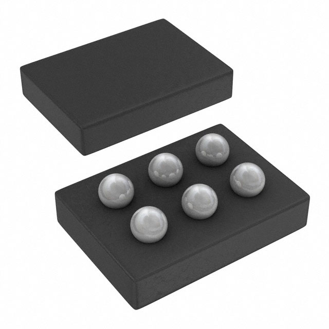
Texas Instruments_CSD25211W1015

Texas Instruments
CSD25211W1015  
Single FETs, MOSFETs

Texas Instruments
CSD25211W1015
278-CSD25211W1015
Ersa
Texas Instruments-CSD25211W1015-datasheets-7110566.pdf
MOSFET P-CH 20V 3.2A 6DSBGA
In Stock : 3683

Not available to buy online? Want the lower wholesale price? Please Send RFQ to get best price, we will respond immediately

QUICK RFQ
ADD TO RFQ LIST
ersa FreeSample ersa flow
  • Quantity
  • Unit Price
  • Ext. Price
    • 1+
    • $0.37260
    • $0.37
    • 10+
    • $0.29477
    • $2.95
    • 30+
    • $0.25668
    • $7.7
    • 100+
    • $0.22356
    • $22.36
    ADD TO CART
    QUICK ORDER
    $0.37260    $0.37
    ISO9001
    Quality Policy
    ISO45001
    ISO14001

    CSD25211W1015 Description

    The Texas Instruments CSD25211W1015 is a highly integrated, high voltage, monolithic smart power switch designed for use in a wide range of applications. It is a member of the Cap-Touch™ family of products, which are designed to provide a highly accurate and reliable method of detecting touch input in a variety of environments.

    Description:

    The CSD25211W1015 is a compact, low-profile, 15-pin, QFN package that is designed to be easily integrated into a variety of electronic systems. It features a high voltage, low noise, and low power consumption, making it ideal for use in battery-powered applications.

    Features:

    • High voltage operation: The CSD25211W1015 is capable of operating at voltages up to 28V, making it suitable for use in a wide range of applications.
    • Low noise: The device is designed to minimize electrical noise, which can be a problem in sensitive applications.
    • Low power consumption: The CSD25211W1015 is designed to operate with low power consumption, making it ideal for use in battery-powered applications.
    • Integrated self-test: The device includes an integrated self-test feature that allows for easy detection of faults and malfunctions.
    • Wide range of capacitive sensing options: The CSD25211W1015 can be used to detect a wide range of touch inputs, including button presses, proximity detection, and gesture recognition.
    • Small form factor: The device is available in a compact, low-profile, 15-pin, QFN package, making it easy to integrate into a variety of electronic systems.

    Applications:

    The CSD25211W1015 is suitable for use in a wide range of applications, including:

    • Industrial control systems
    • Medical equipment
    • Consumer electronics
    • Automotive systems
    • Appliance controls
    • Gaming systems
    • Touch-based user interfaces

    In summary, the Texas Instruments CSD25211W1015 is a highly integrated, high voltage, monolithic smart power switch that is designed for use in a wide range of applications. It offers a high level of accuracy and reliability, along with a compact form factor and low power consumption, making it an ideal choice for a variety of touch-based applications.

    Tech Specifications

    Configuration
    Typical Turn-Off Delay Time (ns)
    Input Capacitance (Ciss) (Max) @ Vds
    Gate Charge (Qg) (Max) @ Vgs
    Typical Rise Time (ns)
    PPAP
    Channel Mode
    Typical Turn-On Delay Time (ns)
    Product Status
    Automotive
    Drain to Source Voltage (Vdss)
    Supplier Package
    Package / Case
    Technology
    REACH Status
    Channel Type
    EU RoHS
    Maximum Continuous Drain Current (A)
    Moisture Sensitivity Level (MSL)
    Operating Temperature
    Maximum Drain Source Voltage (V)
    ECCN
    Mounting Type
    Rds On (Max) @ Id, Vgs
    Standard Package Name
    Vgs(th) (Max) @ Id
    Pin Count
    Mounting
    Lead Shape
    Current - Continuous Drain (Id) @ 25°C
    Typical Gate to Drain Charge (nC)
    SVHC
    Drive Voltage (Max Rds On, Min Rds On)
    HTSUS
    Package
    Maximum Drain Source Resistance (MOhm)
    Typical Gate Charge @ Vgs (nC)
    Typical Input Capacitance @ Vds (pF)
    Category
    PCB changed
    HTS
    FET Type
    Number of Elements per Chip
    ECCN (US)
    Maximum Power Dissipation (mW)
    Supplier Device Package
    Minimum Operating Temperature (°C)
    Maximum Operating Temperature (°C)
    Power Dissipation (Max)
    Typical Fall Time (ns)
    Process Technology
    Package Height
    Mfr
    Vgs (Max)
    RoHS Status
    Typical Gate Threshold Voltage (V)
    FET Feature
    Maximum Gate Source Voltage (V)
    Package Length
    Series
    Part Status
    Package Width
    Base Product Number
    Unit Weight
    Id - Continuous Drain Current
    Fall Time
    RoHS
    Qg - Gate Charge
    Tradename
    Transistor Type
    Number of Channels
    Typical Turn-On Delay Time
    Height
    Maximum Operating Temperature
    Width
    Rds On - Drain-Source Resistance
    Mounting Style
    Vgs - Gate-Source Voltage
    Typical Turn-Off Delay Time
    Transistor Polarity
    Minimum Operating Temperature
    Vds - Drain-Source Breakdown Voltage
    Rise Time
    Length
    Forward Transconductance - Min
    Vgs th - Gate-Source Threshold Voltage
    Pd - Power Dissipation
    USHTS

    CSD25211W1015 Documents

    Download datasheets and manufacturer documentation for CSD25211W1015

    Ersa CSD25211W1015 Datasheet      
    Ersa DSBGA-6L Carrier Tape Change 28/Oct/2013       Carrier Tape 28/Aug/2018      
    Ersa CSD25211W1015 Datasheet      
    Ersa DSBGA/Usip 14/Sep/2016       Mult Dev Marking Chgs 4/Apr/2023      

    Shopping Guide

    Payment Methods
    Payment Methods include Prepayment TT (bank transfer), Western Union, and PayPal. Customers are responsible for shipping costs, bank charges, customs duties and taxes.
    Shipping Rate
    Shipments are made once a day around 5pm, excluding Sundays. Once shipped, the estimated delivery time is usually 5-7 business days, depending on the courier you choose.
    Delivery Methods
    Provide DHL, FedEx, UPS, EMS, SF Express and Registered Airmail International Delivery Service