
 German
 Japanese
 Portuguese
 Korea
Korea
 Mexico
 Dutch
Dutch


Texas Instruments
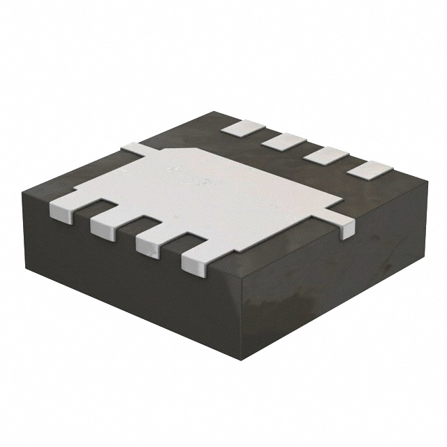
CSD25401Q3

Why Choose Us?
Professional Platform
B2B & B2C purchasingDelivery at full speed
1-2 days deliveryWide variety
Original manufacturers365 days guarantee
Responsible quality
.png)


Tech Specifications
CSD25401Q3 Description
CSD25401Q3 Description
The CSD25401Q3 is a high-performance, single P-Channel MOSFET from Texas Instruments, designed for applications requiring high efficiency and reliability. With a drain-to-source voltage (Vdss) of 20V and a continuous drain current (Id) of 14A at 25°C and 60A at Tc, this MOSFET is well-suited for demanding power management and switching applications. The NexFET™ series offers superior performance and reliability, making it an ideal choice for engineers looking to optimize their designs.
CSD25401Q3 Features
- High Input Capacitance (Ciss): With a maximum input capacitance of 1400 pF at 10V, the CSD25401Q3 provides fast switching and reduced power loss.
- Low Gate Charge (Qg): The maximum gate charge of 12.3 nC at 4.5V ensures efficient gate drive and low power consumption.
- Robust Drain Current: Capable of handling continuous drain currents up to 14A at 25°C and 60A at Tc, making it suitable for high-current applications.
- Low Rds On: With a maximum Rds On of 11.7 mOhm at 10A and 4.5V, the CSD25401Q3 offers low on-resistance and high efficiency.
- Wide Vgs Range: The maximum Vgs of ±12V provides flexibility in gate drive voltage requirements.
- Surface Mount Technology: The surface mount packaging allows for easy integration into compact designs.
- Compliance with Industry Standards: The CSD25401Q3 is REACH unaffected, RoHS3 compliant, and classified under ECCN EAR99, ensuring compliance with environmental and trade regulations.
CSD25401Q3 Applications
The CSD25401Q3 is ideal for a variety of applications where high efficiency, reliability, and performance are critical:
- Power Management: Its high drain current and low on-resistance make it suitable for power supply designs, including battery management systems and power converters.
- Motor Control: The CSD25401Q3's robust performance and low gate charge are ideal for motor control applications, providing efficient switching and reduced power loss.
- Industrial Automation: Its ability to handle high currents and voltages makes it suitable for industrial automation systems, such as motor drives and control circuits.
- Automotive Applications: The CSD25401Q3 can be used in automotive systems, such as electric power steering and battery management, where high reliability and performance are essential.
Conclusion of CSD25401Q3
The CSD25401Q3 from Texas Instruments is a high-performance P-Channel MOSFET that offers superior performance, reliability, and efficiency. Its unique features, such as high input capacitance, low gate charge, and robust drain current, make it an ideal choice for demanding applications in power management, motor control, industrial automation, and automotive systems. While the product is now obsolete, its legacy of performance and reliability continues to be recognized in the industry.
FAQ
Not available to buy online? Want the lower wholesale price? Please Send RFQ to get best price, we will respond immediately


.png?x-oss-process=image/format,webp/resize,h_32)


