
Texas Instruments
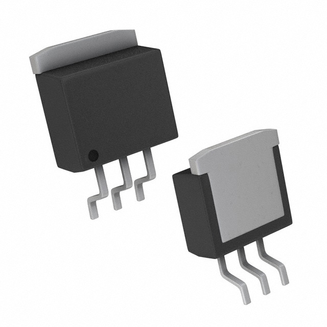
CSD19535KTT
Single FETs, MOSFETs


- 1+
- $3.14474
- $3.14
- 10+
- $2.71915
- $27.19
- 30+
- $2.46578
- $73.97
- 100+
- $2.21076
- $221.08

.png?x-oss-process=image/format,webp/resize,p_30)


CSD19535KTT Description
The CSD19535KTT is a highly-integrated, gate driver solution from Texas Instruments (TI) designed for use in brushless DC (BLDC) motor control applications. This device is part of TI's portfolio of motor control products and is suitable for a wide range of applications, including industrial, automotive, and consumer electronics.
Description:
The CSD19535KTT is a monolithic, synchronous, current-mode, step-down regulator with integrated high-side and low-side gate drivers. It is designed to drive BLDC motors with a wide range of voltage and current requirements. The device is available in a 48-pin QFN (7x7mm) package, making it suitable for compact and space-constrained applications.
Features:
- Integrated high-side and low-side gate drivers: The CSD19535KTT features two gate drivers that can handle high-side and low-side MOSFETs, simplifying the overall motor control design.
- Synchronous step-down regulator: The device operates in a synchronous step-down mode, providing efficient power conversion and reducing power dissipation.
- Wide input voltage range: The CSD19535KTT can handle input voltages from 4.75V to 60V, making it suitable for various power supply scenarios.
- Wide output voltage range: The output voltage range is from 0.95V to 99% of the input voltage, providing flexibility for different motor control applications.
- High efficiency: The device offers high efficiency (up to 98%) under various load conditions, which helps reduce power consumption and improve overall system performance.
- Advanced protection features: The CSD19535KTT includes over-current protection, over-temperature protection, and under-voltage lockout to ensure safe and reliable operation.
- Spread spectrum frequency modulation: This feature helps reduce electromagnetic interference (EMI) and improve system performance.
- Communication interface: The device features a SPI communication interface, allowing for easy configuration and control of the device.
Applications:
- Brushless DC motor control in industrial applications, such as robotics, pumps, and fans.
- Automotive applications, including electric power steering, cooling fans, and window motors.
- Consumer electronics, such as vacuum cleaners, air conditioners, and washing machines.
- Aerospace applications, where high reliability and efficiency are crucial.
- Renewable energy systems, such as solar panel tracking systems and wind turbine control.
In summary, the CSD19535KTT from Texas Instruments is a versatile and efficient gate driver solution for BLDC motor control applications. Its integrated gate drivers, wide input and output voltage ranges, high efficiency, and advanced protection features make it suitable for a wide range of applications across various industries.
Tech Specifications
CSD19535KTT Documents
Download datasheets and manufacturer documentation for CSD19535KTT
 CSD19535KTT
  CSD19535KTT
 Shopping Guide


.png?x-oss-process=image/format,webp/resize,h_32)


