
Texas Instruments
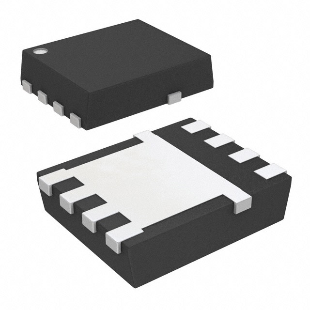
CSD19533Q5AT
Single FETs, MOSFETs


- 1+
- $2.36311
- $2.36
- 10+
- $2.30846
- $23.08
- 30+
- $2.27203
- $68.16

.png?x-oss-process=image/format,webp/resize,p_30)


CSD19533Q5AT Description
The CSD19533Q5AT is a high-performance, single-chip motor controller from Texas Instruments. It is designed for brushless DC (BLDC) motor control in a wide range of applications, including industrial, automotive, and consumer electronics.
Description:
The CSD19533Q5AT is a highly integrated motor controller that combines a gate driver, power MOSFETs, and control logic into a single chip. It uses a proprietary gate drive architecture to provide precise control of the motor's speed and torque. The device also includes advanced protection features to ensure reliable operation in harsh environments.
Features:
- High-Performance Gate Drive: The CSD19533Q5AT uses a proprietary gate drive architecture to provide fast and precise control of the motor's speed and torque.
- Integrated Power MOSFETs: The device includes integrated power MOSFETs, eliminating the need for external components and reducing the overall system cost and complexity.
- Advanced Protection Features: The CSD19533Q5AT includes a range of protection features, including overcurrent, overvoltage, and undervoltage protection, to ensure reliable operation in harsh environments.
- Wide Input Voltage Range: The device can operate from a wide input voltage range of 4.75V to 58V, making it suitable for a wide range of applications.
- Low Power Consumption: The CSD19533Q5AT is designed for low power consumption, making it ideal for battery-powered applications.
Applications:
The CSD19533Q5AT is suitable for a wide range of applications, including:
- Industrial Automation: The device can be used in industrial applications such as robotics, conveyor systems, and pumps.
- Automotive: The CSD19533Q5AT can be used in automotive applications such as electric power steering, windshield wipers, and air conditioning systems.
- Consumer Electronics: The device can be used in consumer electronics such as vacuum cleaners, fans, and air purifiers.
- Medical Devices: The CSD19533Q5AT can be used in medical devices such as infusion pumps and diagnostic equipment.
Overall, the CSD19533Q5AT is a high-performance, single-chip motor controller that offers precise control, advanced protection features, and low power consumption, making it suitable for a wide range of applications.
Tech Specifications
CSD19533Q5AT Documents
Download datasheets and manufacturer documentation for CSD19533Q5AT
 CSD19533Q5A Datasheet
  CSD19533Q5A Datasheet
 Shopping Guide


.png?x-oss-process=image/format,webp/resize,h_32)


