
 German
 Japanese
 Portuguese
 Korea
Korea
 Mexico
 Dutch
Dutch


Texas Instruments
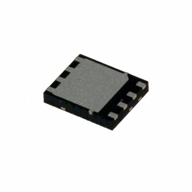
CSD16406Q3

Why Choose Us?
Professional Platform
B2B & B2C purchasingDelivery at full speed
1-2 days deliveryWide variety
Original manufacturers365 days guarantee
Responsible quality
.png)


Tech Specifications
CSD16406Q3 Description
The CSD16406Q3 is a high performance, 16-channel, capacitive touch sensing controller from Texas Instruments. It is designed to provide a highly accurate and reliable solution for capacitive touch sensing applications.
Description:
The CSD16406Q3 is a highly integrated, low power, capacitive touch sensing controller that supports up to 16 capacitive sensing channels. It features a proprietary algorithm that enables it to detect touch events with high accuracy, even in noisy environments. The device also includes a variety of built-in diagnostic and protection features to ensure reliable operation.
Features:
- 16 capacitive sensing channels
- Proprietary algorithm for accurate touch detection
- Low power consumption
- Built-in diagnostic and protection features
- Wide supply voltage range (2.7V to 5.5V)
- Small package size (QFN package)
Applications:
The CSD16406Q3 is suitable for a wide range of applications that require capacitive touch sensing, including:
- Consumer electronics (e.g. smartphones, tablets, remote controls)
- Industrial controls (e.g. touch-based control panels)
- Automotive controls (e.g. infotainment systems, climate control panels)
- Appliance controls (e.g. touch-based oven controls)
- Medical equipment (e.g. touch-based diagnostic equipment)
In summary, the CSD16406Q3 is a highly capable capacitive touch sensing controller that offers high accuracy, low power consumption, and a wide range of features. It is suitable for a variety of applications and is available in a compact package size.
FAQ
| Quantity | Unit Price | Ext. Price |
|---|---|---|
| 1+ | $0.86915 | $0.87 |
| 10+ | $0.74915 | $7.49 |
| 30+ | $0.66515 | $19.95 |
| 100+ | $0.59485 | $59.48 |
Not available to buy online? Want the lower wholesale price? Please Send RFQ to get best price, we will respond immediately


.png?x-oss-process=image/format,webp/resize,h_32)


